Substrate processing device, substrate processing method, and developing device

a substrate processing and substrate technology, applied in the direction of photosensitive materials, instruments, photomechanical equipment, etc., can solve the problems of resisting pattern thereon peeling or collapsing, insufficient washing of the center portion of the centrifugal force, etc., to achieve short time and decrease the effect of development d

Inactive Publication Date: 2008-06-17
TOKYO ELECTRON LTD
View PDF28 Cites 11 Cited by
  • Summary
  • Abstract
  • Description
  • Claims
  • Application Information

AI Technical Summary

Benefits of technology

[0011]The present invention was made under such a situation. An object of the present invention is to provide a technology that allows a development defect to decrease and developing solution to be washed away in a short time.
[0012]Another object of the present invention is to provide a substrate processing apparatus and a substrate processing method that allow rinsing solution to be equally supplied onto a substrate so as to wash away processing solution such as developing solution.
[0013]Another object of the present invention is to provide a substrate processing apparatus and a substrate processing method that allow for example dissolvable substance of resist contained in processing solution or impurities contained in rinsing solution to be prevented from adhering to a substrate.

Problems solved by technology

Thus, the center portion at which the centrifugal force is weak may be insufficiently washed.
If the wafer W is dried with the deposit that adheres on the front surface of the pattern (the front surface of the resist or the front surface of the base material), there is a possibility of which a development defect takes place.
However, in this method, since the centrifugal force at the periphery portion of the wafer W is too strong, there is a possibility of which a resist pattern thereon peels off or collapses.
Moreover, in recent years, semiconductor devices are further becoming miniaturized.
However, there is a problem of which the rinsing solution is not equally replaced with the developing solution.
If surfactant contains impurities such as particles, when the rinsing solution that contains the surfactant is supplied onto the substrate, there is a possibility of which a product defect takes place.

Method used


Image

  • Substrate processing device, substrate processing method, and developing device
  • Substrate processing device, substrate processing method, and developing device
  • Substrate processing device, substrate processing method, and developing device

Examples


first embodiment

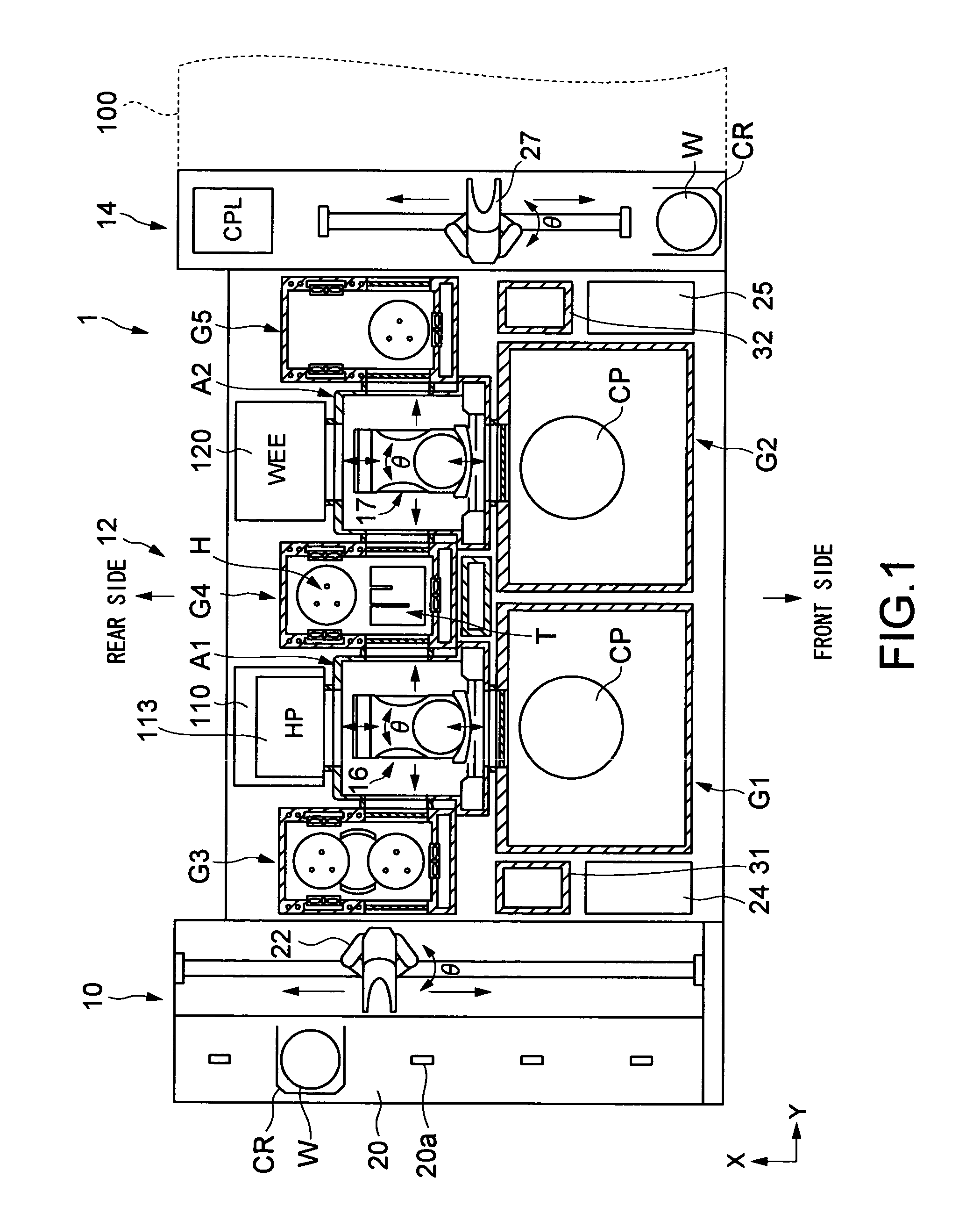
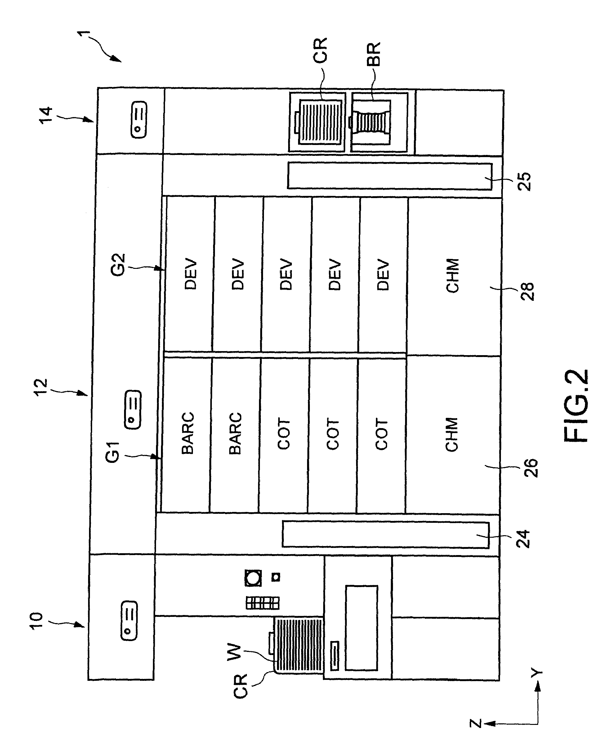
[0103]FIG. 1 to FIG. 3 are schematic diagrams showing an overall structure of a coating / developing processing apparatus according to a first embodiment of the present invention, where FIG. 1 is a plan view and FIG. 2 and FIG. 3 are a front view and a rear view, respectively.

[0104]The coating / developing processing apparatus denoted by reference numeral 1 has a cassette station 10, a processing station 12, and an interface portion 14 that are integrally connected. The cassette station 10 loads and unloads a wafer cassette CR from and to the outside of the apparatus 1. A wafer cassette CR contains a plurality of semiconductor wafers W, for example 25 wafers W. In addition, the cassette station 10 loads and unloads a wafer W to and from a wafer cassette CR. The processing station 12 has single-wafer processing units that are multiply piled at predetermined positions and that perform predetermined processes for wafers W one by one at coating / developing steps. The interface portion 14 tra...

second embodiment

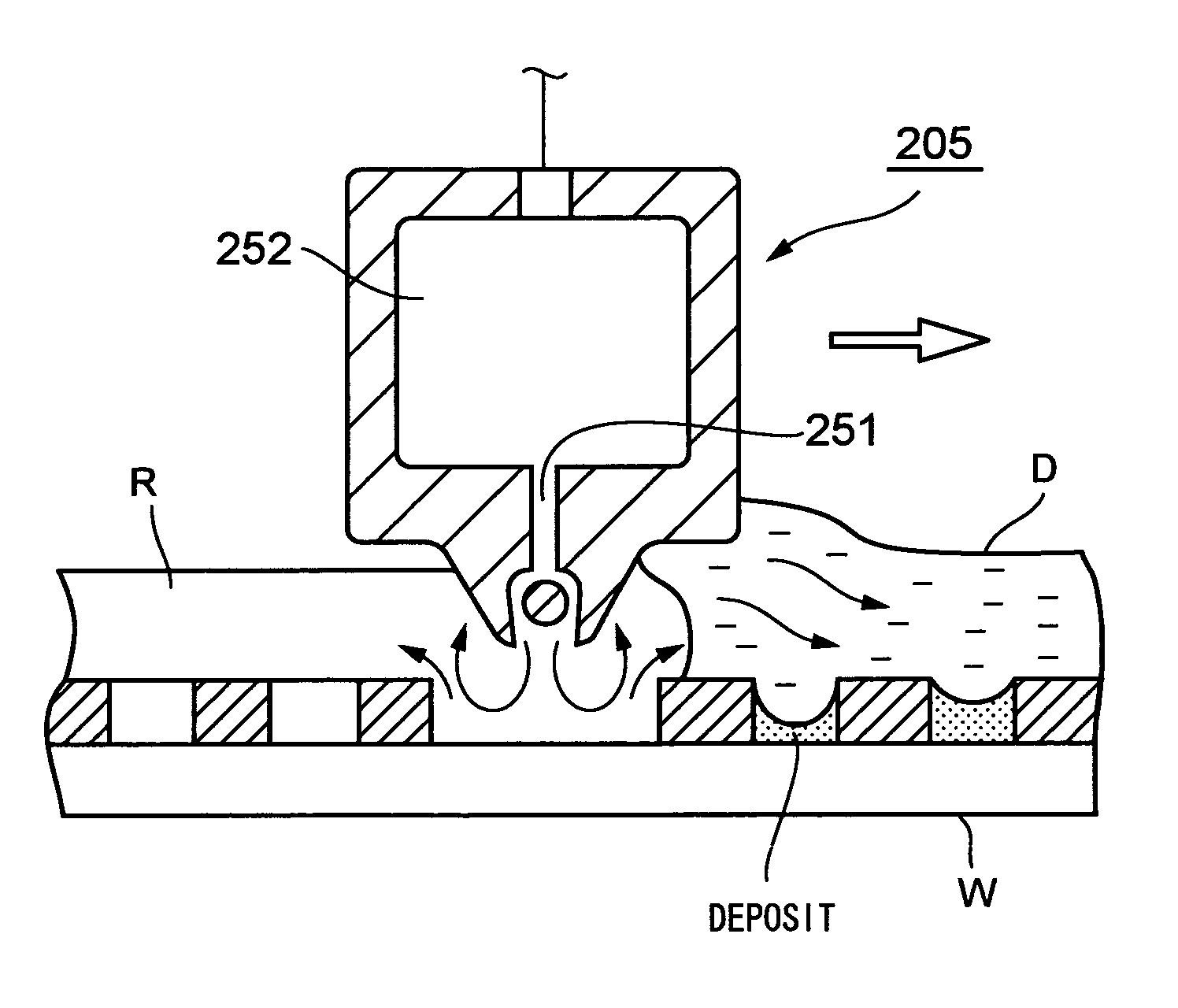
[0156]Next, a second embodiment of the present invention will be described. FIG. 19 is an outlined sectional view showing a developing apparatus and FIG. 20 is an outlined plan view thereof. In the drawings, reference numerals 202 represents a spin chuck that vacuum-sucks and almost horizontally holds the center portion on the rear side of for example an 8-inch wafer W as a substrate. The spin chuck 202 is structured so that it is rotated, raised, and lowered by a driving portion 220. While the wafer W is being sucked and held by the spin chuck 202, an outer cup 230 and an inner cup 231 surround the periphery of the wafer W. An upper cylinder portion of the inner cup 231 is inclined inwardly so that an upper opening portion thereof is narrower than a lower opening portion thereof. When the outer cup 230 is raised and lowered by a raising / lowering portion 232, the inner cup 231 is raised and lowered in a part of the moving range of the outer cup 230. A disc 233 that surrounds a rotat...

third embodiment

[0167]Next, a third embodiment of the present invention will be described. According to the third embodiment, air supplying means is added to the washing solution supplying nozzle 205 shown in FIG. 22. The discharging opening 250 of the nozzle 205 according to the present embodiment is longer than that according to the foregoing embodiments. As shown in FIG. 25, the air supplying means has a blowing opening 270 that blows gas, for example air, to the front surface of the wafer W. The blowing opening 270 is disposed at a side wall portion in the moving direction of the washing solution supplying nozzle 205. The blowing opening 270 is disposed above the surface of the developing solution D. The blowing opening 270 is inclined against the axial line (discharging direction) of the discharging opening 250 by an angle of .theta., for example 0° to 60°. In addition, the blowing opening 270 is composed of a plurality of air supplying holes each having a diameter of 0.4 mm. The air supplying...


PUM

PropertyMeasurementUnit
distanceaaaaaaaaaa
distanceaaaaaaaaaa
temperatureaaaaaaaaaa

Abstract

Rinsing nozzles 310a to 310e are moved on a wafer W while they are discharging rinsing solution 326. At that point, discharging openings 317a to 317e are contacted to developing solution 350 coated on the wafer W or rinsing solution 326 on the wafer W. Thus, the impact against the wafer W can be suppressed. As a result, pattern collapse can be prevented. In addition, a front portion of the developing solution 350 can push away the developing solution 350.

Description

TECHNICAL FIELD[0001]The present invention relates to a substrate processing apparatus and a substrate processing method for performing a developing process for a semiconductor substrate at a photolithography step for producing a semiconductor device and to a developing apparatus for performing a developing process using developing solution for a substrate on which resist has been coated and a developing process has been performed.BACKGROUND OF THE INVENTION[0002]At a photolithography step upon production of a semiconductor device, photoresist is coated on the front surface of a semiconductor wafer (hereinafter referred to as “wafer”). Thereafter, a mask pattern is exposed on the resist and developed. As a result, a resist pattern is formed on the front surface of the wafer.[0003]At such a photolithography step, the developing process is performed by for example a paddle method or a dip method. In the paddle method, developing solution is supplied to a wafer. On the other hand, in t...

Claims


Application Information

Patent Timeline
Patent Type & Authority Patents(United States)
IPC IPC(8): H01L21/302G03F7/30H01L21/00
CPCG03F7/30G03F7/3021H01L21/67225H01L21/67178H01L21/67184H01L21/6715G03F7/3057
Inventor AWAMURA, TETSUTOSHIKIBA, YUKIOTANAKA, KEIICHIOKUBO, TAKAHIRONISHIKIDO, SHUUICHI
Owner TOKYO ELECTRON LTD
Why Eureka
Try Eureka