Wafer level packaging process

a packaging process and wafer technology, applied in the direction of brassieres, semiconductor devices, semiconductor/solid-state device details, etc., can solve the problems of increased difficulty/cost of the via process, large parasitic capacitance, cross-talk and substantial interconnection resistance,

Active Publication Date: 2008-07-01
MAXIM INTEGRATED PROD INC
View PDF12 Cites 52 Cited by
  • Summary
  • Abstract
  • Description
  • Claims
  • Application Information

AI Technical Summary

Benefits of technology

[0018]Another objective of this invention is to package the devices / structures with a controllable cap gap between one of the device / structure surfaces and the cap electrode. This is important for MEMS structures since additional control flexibility is introduced which will result in improved performance and reliability. By way of example, a controlled cap gap may be used to provide motion limits (mechanical stops) and / or electrostatic drivers for imparting motion to a MEMS device.
[0019]Still another objective of this invention is to form a mechanical structure with minimized thermal-stresses due to thermal expansion mismatch between substrate and the filled metal(s) / alloy. As metals usually have much higher thermal expansion than silicon or glass, vias filled with solid metal plug / stud may encounter very high thermal stress problems or even changing surface height / roughness on top of the via, which will cause a variable top surface and thus non-stable performance.

Problems solved by technology

Wafer level packaging of micro-electro-mechanical system (MEMS) devices has been an attractive and challenging topic in recent years.
The feed-through lines crossing the bond rim usually don't allow a metal-related bond.
However, this lateral lead-out has relatively long feed-through lines, which leads to large parasitic capacitances, cross-talk and substantial interconnection resistances.
For reasonably large format wafer processes (e.g., 4-inch or 6-inch above), a wafer with vias calls for substrate rigidity (i.e., wafer thickness) that increases the difficulty / cost of the via process, and also leads to high parasitic coupling capacitances.
This process starts the glass wafer with via forming before bonding to another substrate, hence the rigidity of the glass wafer becomes a problem.
Normally thin glass of around 150 um thick is used in a small wafer format (e.g., no more than 3-inch), as forming through vias on a thicker wafer will tremendously increase the process difficulty and thus the fabrication cost, and also increases the parasitic capacitances and cross-talk between feed-through paths.
Some of the required process steps, like the dielectric filling, polishing and recessing, and final dielectric membrane releasing, etc., increases the process difficulty and may lead to a stress issue.
This might cause thermal stress issue due to the large thermal mismatch between substrate and metal(s) and hence device reliability issue.

Method used


Image

  • Wafer level packaging process
  • Wafer level packaging process
  • Wafer level packaging process

Examples


first embodiment

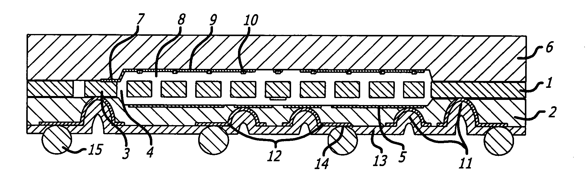
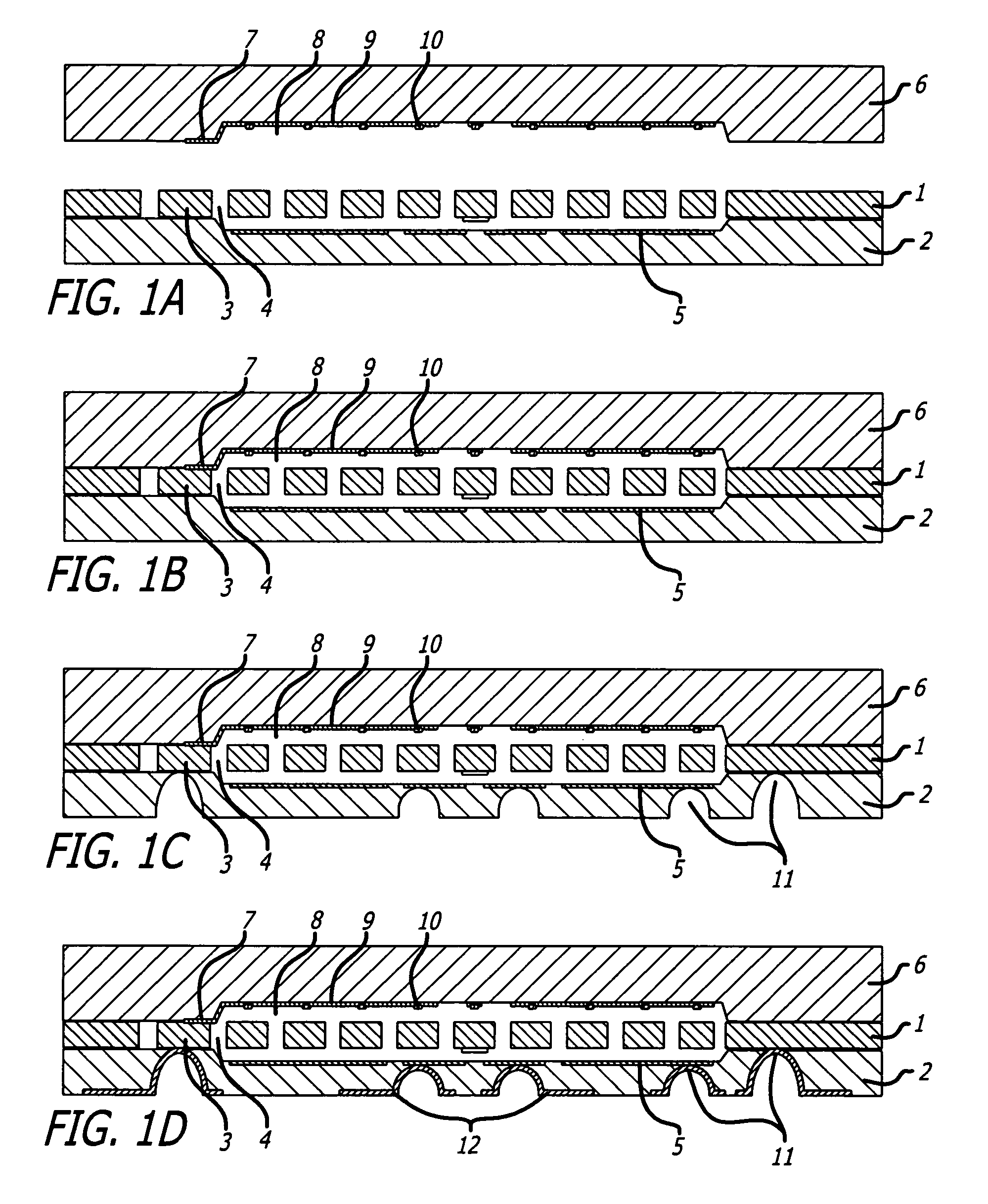
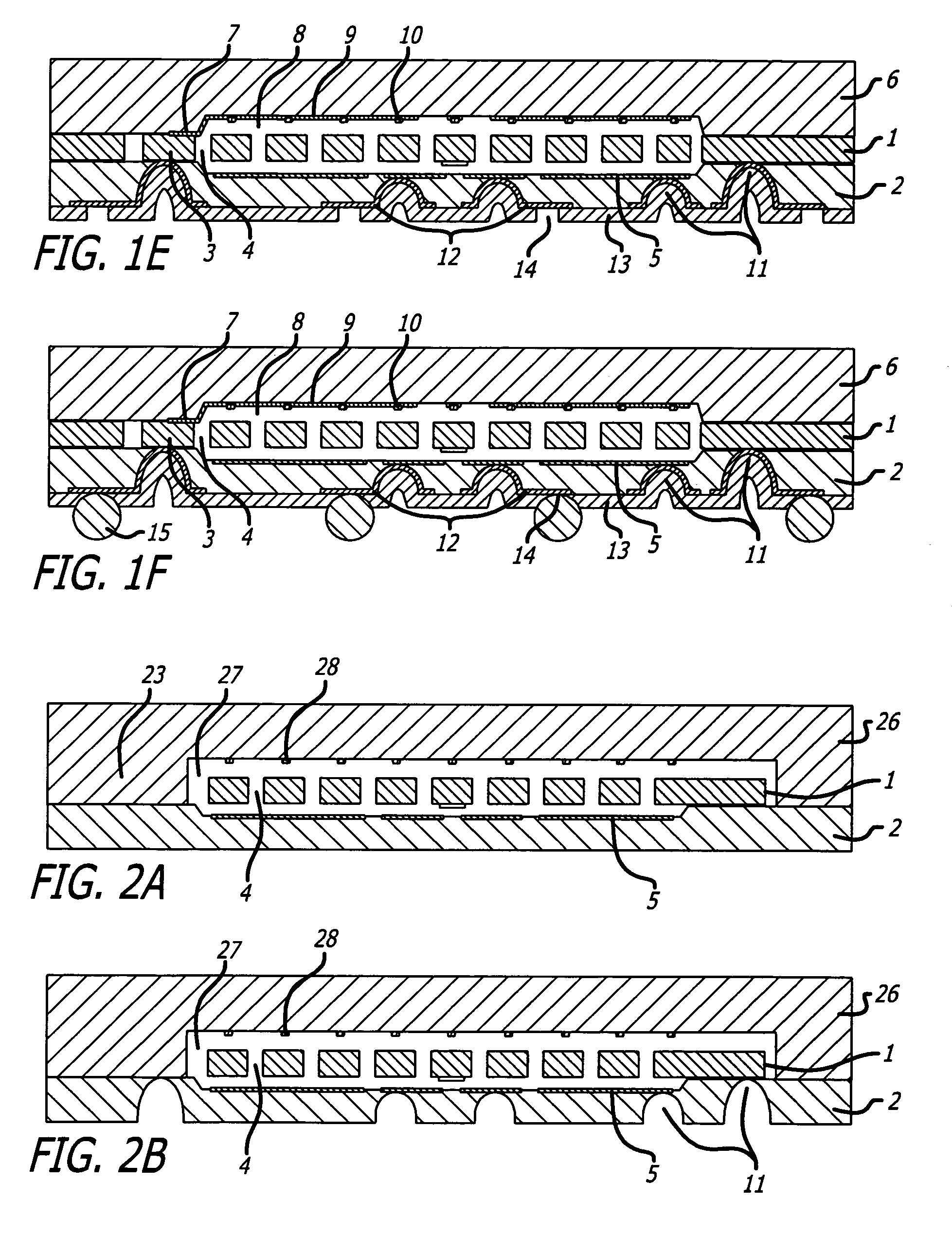
[0020]the invented wafer level package fabrication process is illustrated in FIGS. 1a through 1f. The DEVICE 1 to be packaged may be a MEMS device, an integrated circuit or some other device, hereafter simply a DEVICE, normally of silicon, mounted on a substrate 2 (e.g., in this embodiment, glass), as shown in FIG. 1a. The electrically conductive regions to lead outs 5 can be, by way of example, doped silicon, metal, an alloy layer or stack on substrate 2 or DEVICE 1 or both, or a combination of such materials. As shown in FIG. 1b, the outer surface of DEVICE 1 can be bonded with another glass cap wafer 6. The bonding surface can be formed by either a fine polishing after thinning (e.g., grinding, milling or etching) of the DEVICE layer 1, or an etch stop layer buried in the original DEVICE substrate, or a fine control of the DEVICE layer thinning process, or just planar processes on substrate 2. Isolated conductive island 3 is formed by a DEVICE layer etch process where through tre...

third embodiment

[0029]this invention is illustrated in FIGS. 3a through 3h. In FIG. 3a, a DEVICE wafer 101 bonded with a cap wafer 201 with a cap gap 203 is the starting material (FIG. 3a). On DEVICE wafer 101, metal pads 106 are located on top of an optional dielectric layer 104 as usual. DEVICE structure 103 and optional passivation layer 102 are on top side of the wafer. Optional thin metal feed-through 105 is led out to the bonding interface where optional cap electrode 202 is led to and electric connection is made by press-on bonding of metals. A DEVICE wafer 101 backside thinning is optionally performed prior to via processing.

[0030]The via process starts with backside holes 107 formed in the DEVICE substrate wafer as shown in FIG. 3b. If DEVICE wafer 101 is silicon, this can be done by a masked etch including deep reactive ion etch (DRIE) or an anisotropic etch (e.g., KOH or TMAH etch). In the case of a glass DEVICE wafer 101, this can be a combined process of etch / drill / mill / water jet / sand ...


PUM


Abstract

Wafer level packaging process for packaging MEMS or other devices. In some embodiments, a MEMS wafer with normal thickness is firstly bonded to a cap wafer of normal thickness, followed by a thinning on the backside of the MEMS wafer. After this, the bonded wafer stack and the capping of the hermetically packaged MEMS devices are still rigid enough to do further processing. On this basis, through vias on the thinned substrate can be easily formed and stopped on the regions to be led out (e.g., metal pads / electrodes, highly doped silicon, etc.). Vias can be partially filled as this is the final surface of process. Even thick metal coated / patterned vias have much more space to relax possible thermal stress, as long as the vias are not completely filled with hard metal(s). Various embodiments are disclosed.

Description

BACKGROUND OF THE INVENTION[0001]1. Field of the Invention[0002]The present invention relates to the field of wafer level packaging.[0003]2. Prior Art[0004]Wafer level packaging of micro-electro-mechanical system (MEMS) devices has been an attractive and challenging topic in recent years. A hermetic package can greatly improve the device performance and reliability. Consequently, hermetic bonding is highly preferred in many MEMS devices. Bonding techniques used in the field have included adhesives / polymer / epoxy bond (which are not hermetic bonds), solder eutectic bonds, Si / metal eutectic bonds, metal-metal thermal compression bonds, glass frit bonds, anodic bonds, etc.[0005]A common way of providing electrical lead-outs is through lateral feed-through lines to the edge of the die, which is then sealed by a cap wafer bonded over the die. The feed-through lines crossing the bond rim usually don't allow a metal-related bond. Instead, a dielectric-bond is necessary in this arrangement. ...

Claims


Application Information

Patent Timeline
Patent Type & Authority Patents(United States)
IPC IPC(8): H01L21/46H01L21/301H01L21/78
CPCB81C1/00301B81B2207/096H01L21/76898H01L2224/11
Inventor SRIDHAR, UPPILIZOU, QUANBO
Owner MAXIM INTEGRATED PROD INC
Why Eureka
Try Eureka