
Semiconductor circuit, operating method for the same, and delay time control system circuit

a control system and circuit technology, applied in pulse manipulation, pulse technique, instruments, etc., can solve the problems of delay time recalculation, re-extraction, and overheads of rerouting, and achieve the effect of reducing the number of delays

Inactive Publication Date: 2008-07-01
KK TOSHIBA
View PDF11 Cites 15 Cited by
  • Summary
  • Abstract
  • Description
  • Claims
  • Application Information

AI Technical Summary

Benefits of technology

The present invention relates to a semiconductor circuit and a delay time control system. The semiconductor circuit includes a first buffer and a plurality of capacitances connected in parallel between a fixed potential and a current flow path. The delay time control system includes a plurality of control terminals connected in series with the capacitances and a memory. The control terminals control the connection between the capacitances and the output pad, allowing for external adjustment of delay time. The technical effects of the invention include improved delay time control and improved performance of semiconductor circuits.

Problems solved by technology

Therefore, troublesome overheads of rerouting, re-extraction, delay time recalculation and the like occur.
Furthermore, not only can the effects of that adjustment not be known until executed, but there may be adverse affects to other portions as well.
Moreover, this adjustment method can basically only increase delay, and is equivalent to not having an adjustment method for reducing delay.
Even if this constraint is imposed on a conventional engineering design (EDA) tool, it is difficult to be satisfied, thereby requiring manual fine adjustment by analyzing the results from that tool.
However, since the buffer delay value of the primitive cell is about 100 to 200 ps according to a 130 nm process, signal arrival time cannot be delayed by adding a buffer.
Thus, delay needs to be adjusted by deliberately diverting interconnects, which increases interconnect capacitance.
Relaxing constraints may cause wider margins and a decrease in yield, and restarting from routing delays design completion.

Method used


Image

  • Semiconductor circuit, operating method for the same, and delay time control system circuit
  • Semiconductor circuit, operating method for the same, and delay time control system circuit
  • Semiconductor circuit, operating method for the same, and delay time control system circuit

Examples


first embodiment

(Variable Capacitance Embedded Buffer)

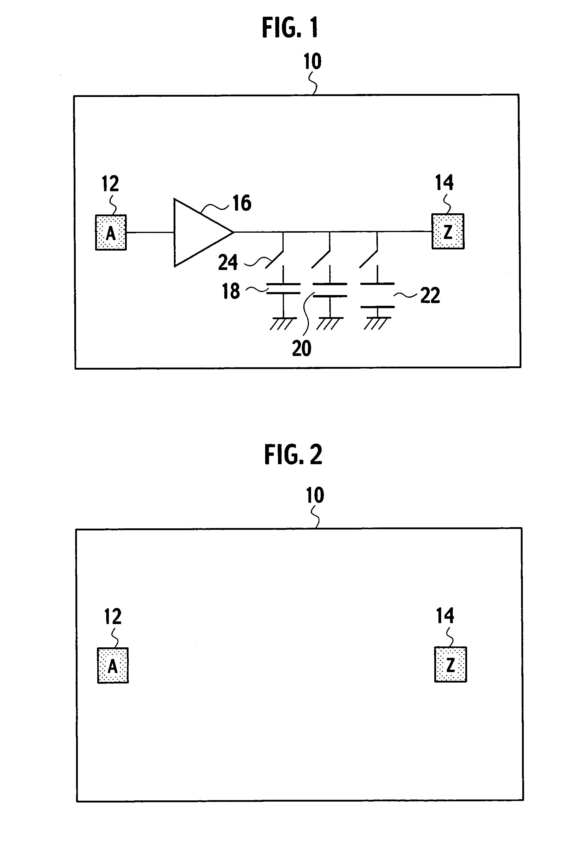
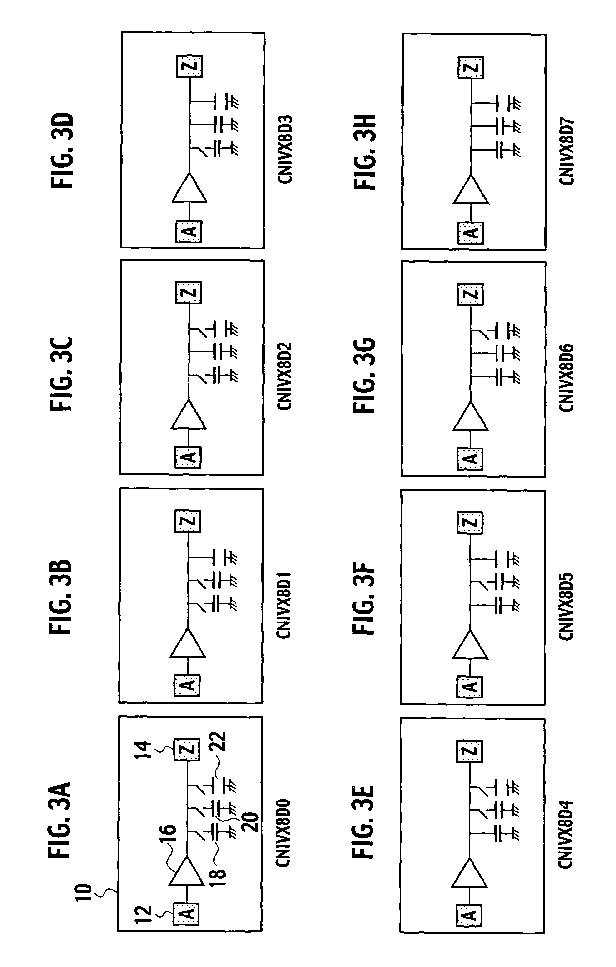
[0086]As shown in FIG. 1, in a semiconductor circuit according to a first embodiment of the present invention, a schematic circuitry of a variable capacitance embedded buffer 10 includes: a buffer 16; an input pad (A) 12 connected to the input terminal of the buffer 16; an output pad (Z) 14 connected to the output terminal of the buffer 16; and multiple capacitances 18, 20, and 22 positioned on the output side of the buffer 16, respectively, differ in value, and can be mutually connected in parallel. Adjustment of delay time of the variable capacitance embedded buffer 10 is possible by controlling the connection between each of the multiple capacitances 18, 20, and 22 and the output pad (Z) 14.

[0087]Alternatively, switches 24 connected between the output pad (Z) 14 and each of the multiple capacitances 18, 20, and 22 and which control the connection therebetween, may be provided.

[0088]The example of FIG. 1 has three capacitances 18, 20, and 22; ...

example 1

[0106]When delays from the PLL 36 to the clock terminal CK of the F / F A30 and from the PLL 36 to the clock terminal CK of the F / F B32 are both 3.456 ns, the skew is 0 ns.

example 2

[0107]When a delay from the PLL 36 to the clock terminal CK of the F / F A30 is 3.456 ns and delay from the PLL 36 to the clock terminal CK of the F / F B32 is 3.000 ns, the skew is −0.456 ns.


PUM


Abstract

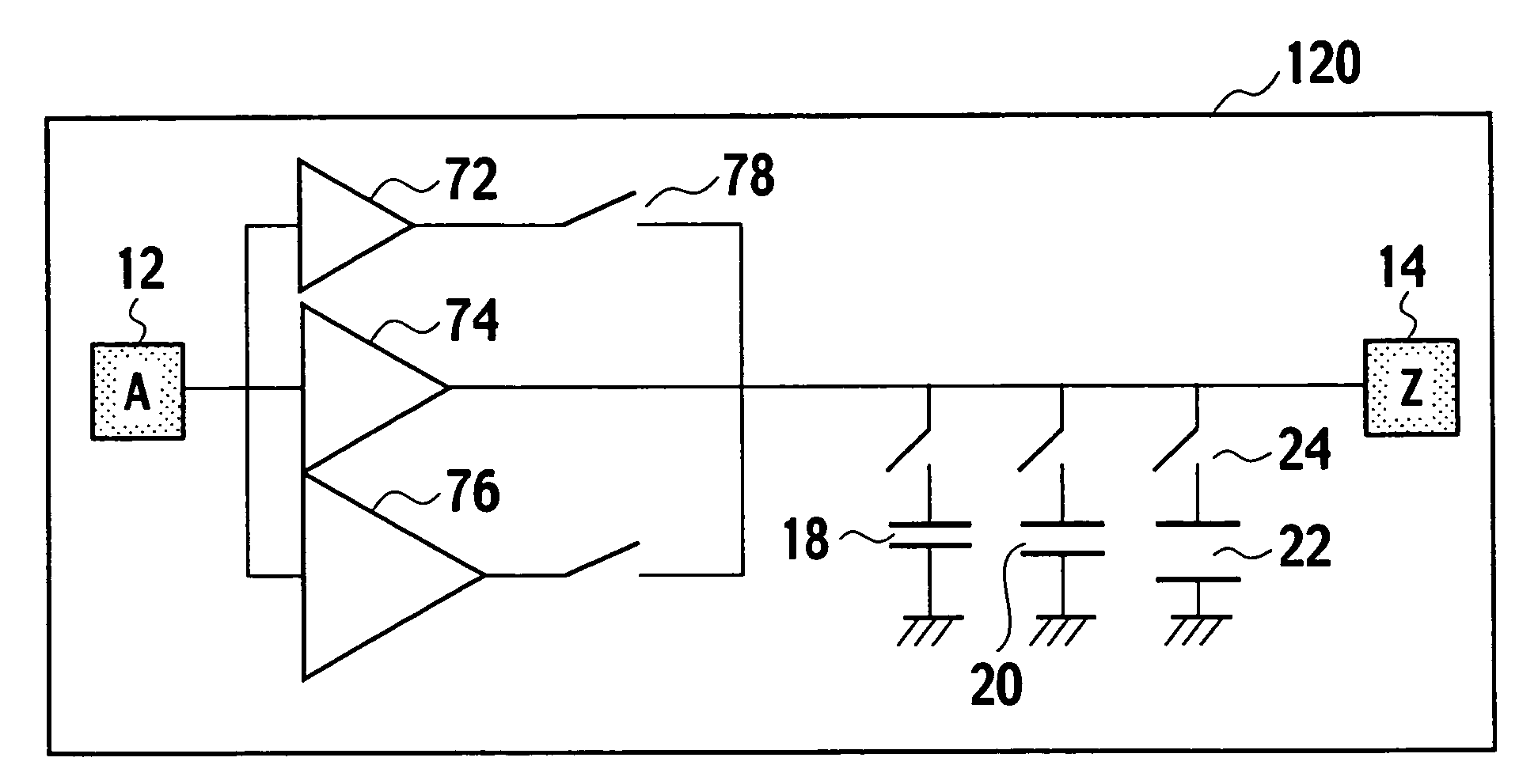
A semiconductor circuit allows a timing adjustment after detailed routing without rearrangement and rerouting, an adjustment of delay variance due to process variation, and a delay adjustment even after chip formation using a primitive cell with a built-in means for adjusting delay time. The circuit connected between an input pad and an output pad, an operating method for the same, and a delay time control system circuit, which externally adjusts delay time of a plurality of control terminal-equipped / variable capacitance embedded buffers configures a semiconductor circuit. The structure includes: a first buffer connected between the input pad and the output pad; and a plurality of capacitances connectable in parallel between a fixed potential and a current flowing path, which is positioned between the first buffer and the output pad, and that controls connection between each of the plurality of capacitances and the output pad.

Description

CROSS REFERENCE TO RELATED APPLICATIONS AND INCORPORATION BY REFERENCE[0001]This application is based upon and claims the benefit of priority from prior Japanese Patent Application P2004-365568 filed on Dec. 17, 2004; the entire contents of which are incorporated by reference herein.BACKGROUND OF THE INVENTION[0002]1. Field of the Invention[0003]The present invention relates to a semiconductor circuit. More specifically, it relates to a semiconductor circuit, which allows a timing adjustment after detailed routing without rearrangement and rerouting by using primitive cells (variable delay cells) including a built-in means that adjusts delay time, and which is utilized for cell-based designs.[0004]2. Description of the Related Art[0005]In a conventional synchronous dynamic random access memory (SDRAM), data writing and reading can be successively performed in sync with an external clock while switching banks, which are provided by dividing a memory cell array into multiple banks. Fu...

Claims


Application Information

Patent Timeline
Patent Type & Authority Patents(United States)
IPC IPC(8): H03H11/26G11C11/407G11C11/4093H03K5/13
CPCH03K5/133H03K2005/00058H03K2005/00071
Inventor SHIMAZAWA, TAKAYOSHI
Owner KK TOSHIBA
Learn More