Germanium silicon heterostructure photodetectors

a heterostructure, germanium silicon technology, applied in the field of semiconductor photodetectors, can solve the problems of affecting the reliability of germanium contact, affecting the quality of germanium contact, and the difficulty in integrating germanium into the standard silicon cmos process, etc., to achieve good electrical contact

Active Publication Date: 2008-07-08
CISCO TECH INC
View PDF1 Cites 185 Cited by
  • Summary
  • Abstract
  • Description
  • Claims
  • Application Information

AI Technical Summary

Benefits of technology

[0009]In some examples according to the current invention, the germanium collection region is established over a p-type doped silicon region and outdiffusion from the silicon region dopes a portion of the germanium, thereby establishing good electrical contact. Establishing a physical contact to the p-type doped silicon using standard CMOS technology enables the establishment of electrical contact to the germanium silicon avalanche detector without requiring the establishment of a physical contact to the germanium material.

Problems solved by technology

However, some challenges remain.
For example, in some cases, the unique combination of Ge and Si can be exploited to improve the sensitivity of optical receivers operating in the near infra-red (NIR) regime due to the absorption properties of germanium in conjunction with the carrier multiplication properties of silicon; however, incorporating germanium into the standard silicon CMOS processes can be problematic.
For example, the standard CMOS technology for establishing a contact to silicon material isn't as effective for reliably establishing a good quality contact to germanium.
Technology gaps related to germanium integration into CMOS processes may hamper the design, development and manufacturability of a variety of new devices.

Method used


Image

  • Germanium silicon heterostructure photodetectors
  • Germanium silicon heterostructure photodetectors
  • Germanium silicon heterostructure photodetectors

Examples


Embodiment Construction

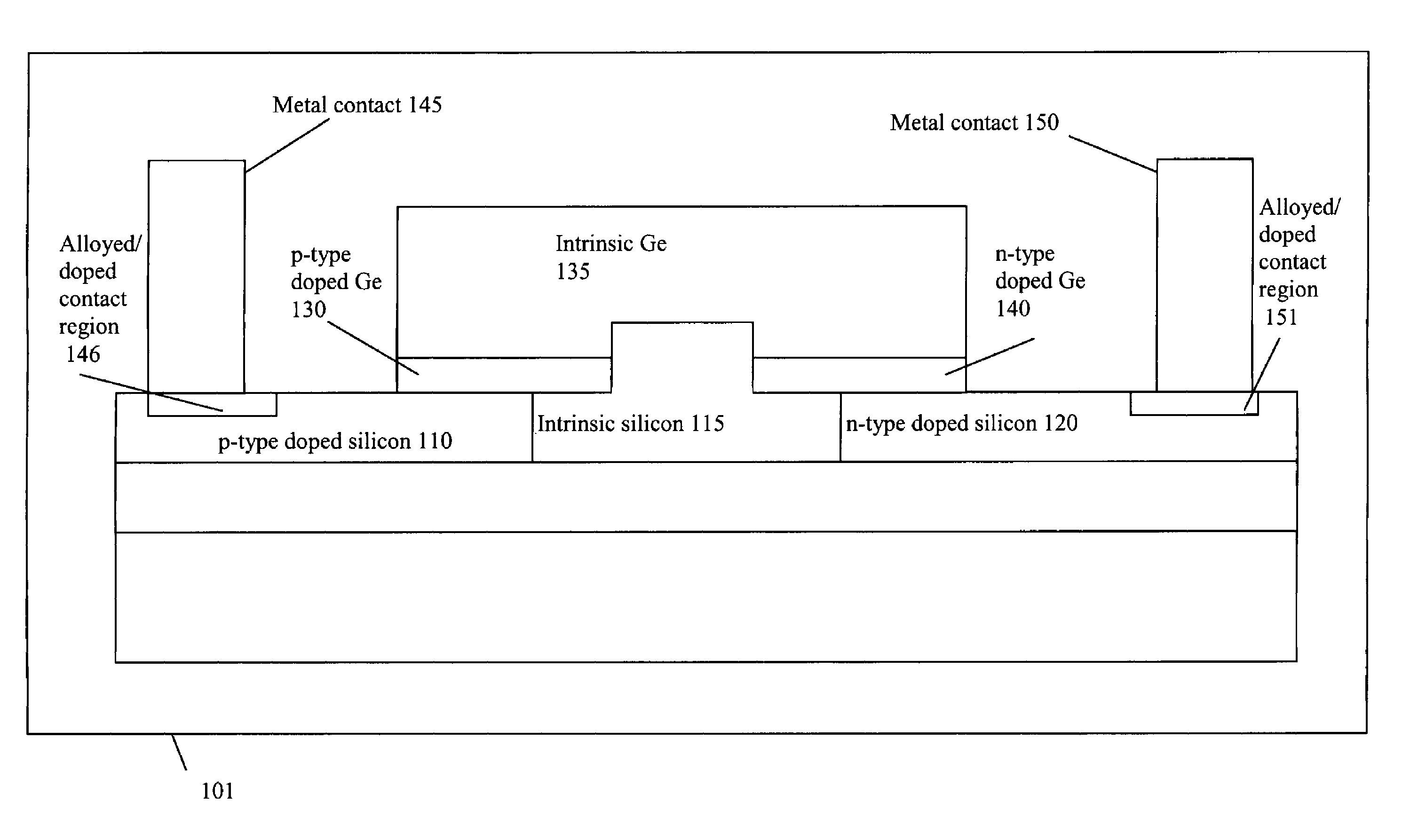
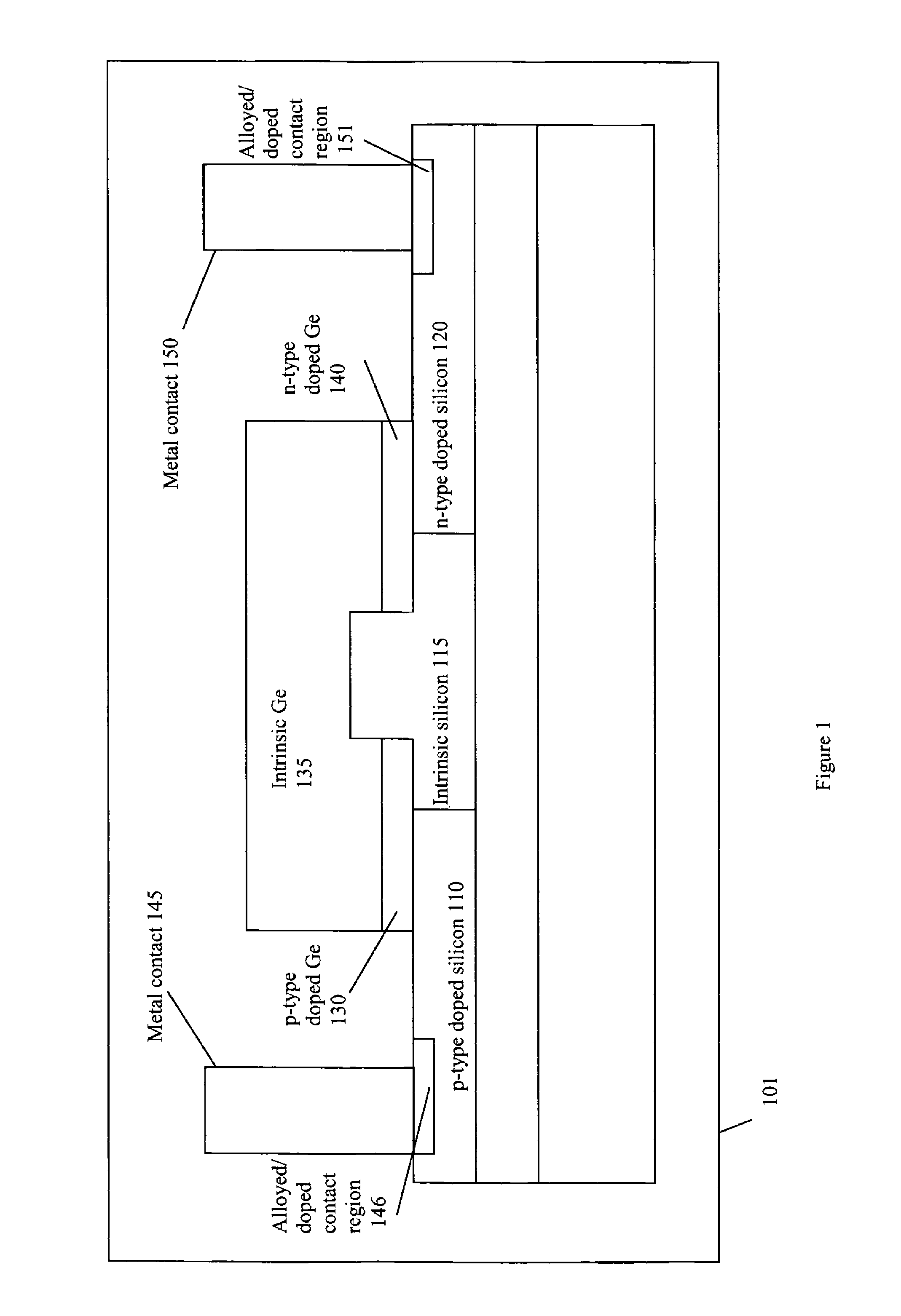
[0029]FIGS. 1 and 2 illustrate examples of horizontal germanium silicon heterostructure photodetectors 101 and 201 according to the current invention. According to the current invention, a horizontal germanium silicon heterostructure photodetector comprises a horizontal germanium p-i-n diode disposed over a silicon p-i-n diode, integrated on a substrate. According to the current invention, an electrical contact is established to the p-type doped region of the silicon p-i-n and another electrical contact is established to the n-type doped region of the silicon p-i-n, thereby enabling electrical coupling to the germanium n-type doped and p-type doped regions without requiring the use of conventional metal contacts to a germanium layer.

[0030]In FIG. 1, the parasitic silicon p-i-n comprises p-type doped silicon 110, intrinsic silicon 115 and n-type doped silicon 120; the germanium p-i-n comprises p-type doped germanium 130, intrinsic germanium 135 and n-type doped germanium 140. Similar...


PUM


Abstract

A horizontal germanium silicon heterostructure photodetector comprising a horizontal germanium p-i-n diode disposed over a horizontal parasitic silicon p-i-n diode uses silicon contacts for electrically coupling to the germanium p-i-n through the p-type doped and n-type doped regions in the silicon p-i-n without requiring direct physical contact to germanium material. The current invention may be optically coupled to on-chip and/or off-chip optical waveguide through end-fire or evanescent coupling. In some cases, the doping of the germanium p-type doped and/or n-type doped region may be accomplished based on out-diffusion of dopants in the doped silicon material of the underlying parasitic silicon p-i-n during high temperature steps in the fabrication process such as, the germanium deposition step(s), cyclic annealing, contact annealing and/or dopant activation.

Description

REFERENCE TO PRIOR APPLICATION[0001]This application claims the benefit under 35 U.S.C. § 119(e) of U.S. Provisional Patent Application No. 60 / 586,205 filed on Jul. 8, 2004, entitled “SAM-APD GeSi Waveguide Photodetector,” which is incorporated by reference herein in its entirety. This application claims the benefit under 35 U.S.C. § 119(e) of U.S. Provisional Patent Application No. 60 / 586,161 filed on Jul. 8, 2004, entitled “Out-diffusion Contacted GeSi Waveguide Photodetector,” which is incorporated by reference herein in its entirety. This application claims the benefit under 35 U.S.C. § 119(e) of U.S. Provisional Patent Application No. 60 / 589,298 filed on Jul. 20, 2004, entitled “Germanium Integration,” which is incorporated by reference herein in its entirety.FIELD OF INVENTION[0002]Invention relates to semiconductor photodetectors, particularly to germanium silicon heterostructure photodetectors.BACKGROUND OF INVENTION[0003]Recent innovations in silicon optoelectronic material...

Claims


Application Information

Patent Timeline
Patent Type & Authority Patents(United States)
IPC IPC(8): H01L31/00
CPCH01L31/028H01L31/1812H01L31/1075Y02E10/547G02B6/4295H01L31/022408H01L31/105
Inventor MASINI, GIANLORENZOGUNN, III, LAWRENCE C.CAPELLINI, GIOVANNI
Owner CISCO TECH INC
Why Eureka
Try Eureka