[0011]On the basis of the prior art it is the object of the present invention to provide a possibility of producing contacts between a chip and the antenna of a contactless chip card in a simple and particularly fast manner, whereby said contacts are to be extremely electrically and mechanically reliable.
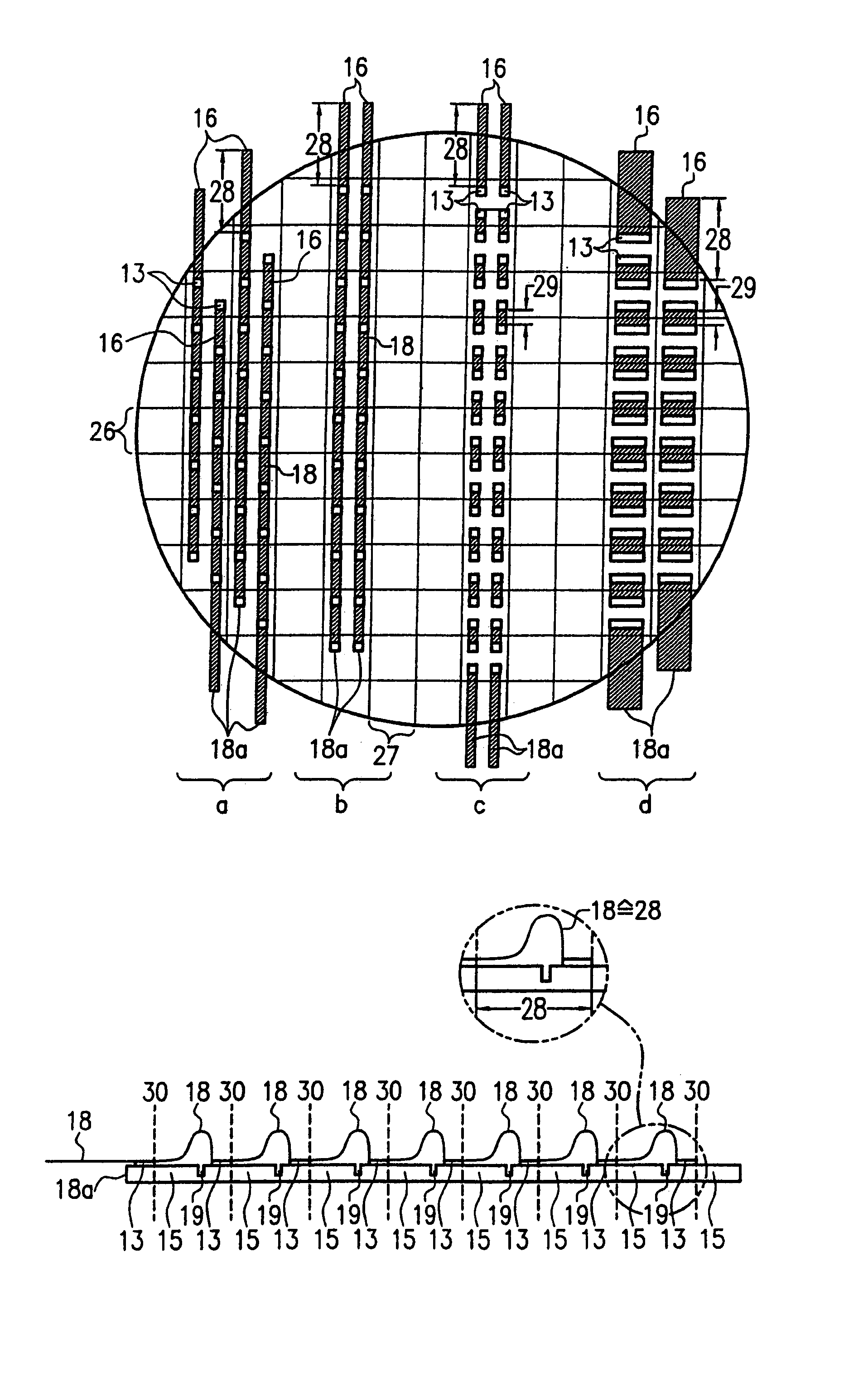
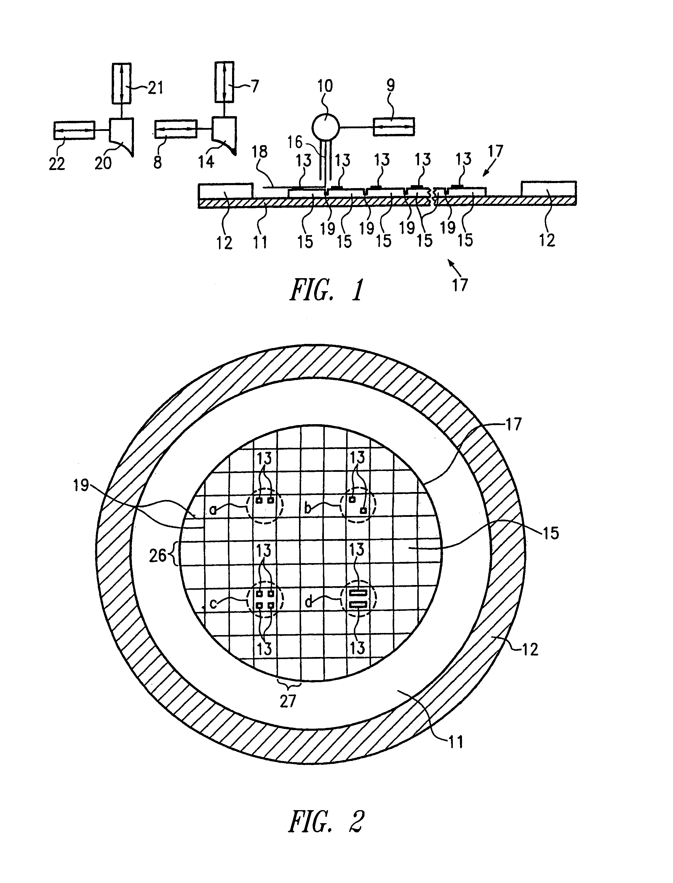
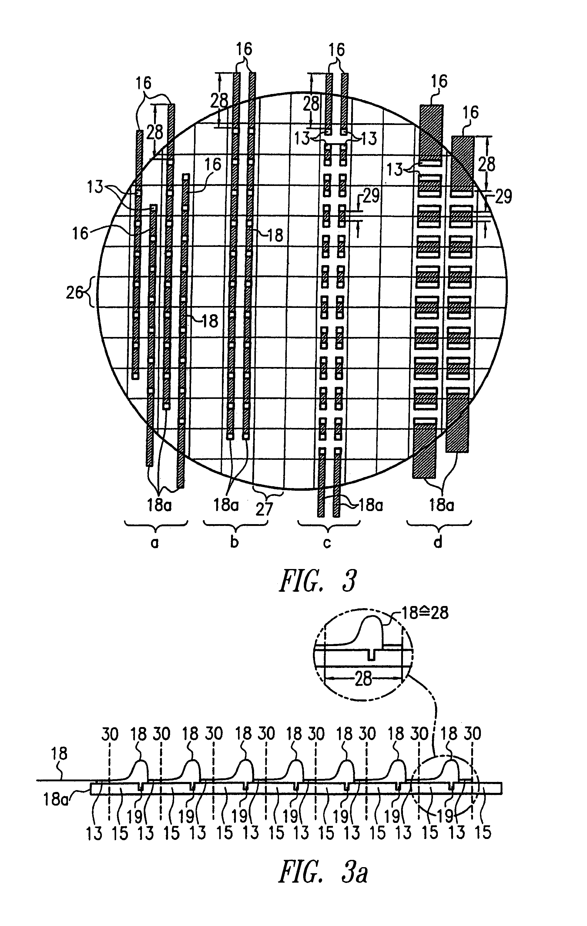
[0016]In accordance with a special aspect of the present invention, chip
contact element units are produced on a
wafer level, whereby said units serve to provide an
electrical connection between the “naked” chip and a loop conductor or antenna disposed in a chip card body. The contact elements are thereby preferably terminal lugs, which are directly connected with the bond pads of the chip on a
wafer level. The contact elements preferably provided as terminal lugs have dimensions allowing a contact with the contact terminals of loop conductors or antennas without involving any problems, wherein the overall construction height of the chip card is at most unessentially increased due to the evenly projecting terminal lugs. The length of said contact elements may be so dimensioned that the contact elements permit a connection of the chip with contact terminals disposed at the opposite side of the bond pads of the chip, whereby the turning by means of a
flip chip process described above in connection with the prior art is avoided. The actual contacting with the antenna can be effected extremely easily and fast.
[0017]Apart from the above-described advantages the
present method especially has the
advantage that an efficient production of chip
contact element units already on a wafer level is achieved, so that a laborious individual bonding of each individual chip is no longer necessary. Thus, it is possible to contact whole rows of chips on a wafer at the same time, and in the case where the individual rows of the waver are arranged to have the correct distance to one another in advance, even a simultaneous bonding of all bond pads of the chip with a foil placed over the chips of the wafer can be achieved. During the production of said chip
contact element units the chips remain grouped to each other, whereby said grouping essentially corresponds to the grouping defined by the wafer production, and whereby, of course, a broadening of the distances between the individual chips should be obtained with suitable means. The spreading of the individual chip rows or, respectively, chip columns may thereby be effected by suitable precise mechanical apparatus, whereby an
adhesive foil is preferably used for ensuring the correct alignment.
[0019]The eventually produced chip contact element unit is extremely robust, as the contact elements are resistant to tensile loads due to their dimensions and the bond pads preferably having a corresponding size, with the result that it may no longer be required to glue the chips onto the chip card body, whereby the process times are reduced because of the avoidance of the
retention time required for gluing. Thus, the chip is not connected with the chip card body, which results in an efficient
strain relief of the chip, as the chip card body may be extended or bent without stressing the chip itself. In the case where the chip is to be protected with a cover
mass, the
strain relief may be achieved by the cover
mass being more easily extensible than the chip card body. Moreover, the protection of the chip may also be obtained by means of a cover foil laminated onto the chip and the chip card body, whereby a sticky or
adhesive connection of the cover foil with the chip or the contact elements has to be avoided so as to maintain the aforementioned
strain relief.
[0020]If it is desired to connect the chip with the chip card body, e.g. by means of gluing, the aforementioned strain relief of the chip may be obtained by selecting the bonding glue used between the chip and the chip card body such that the chip is more extensible or, respectively, softer than the chip card body. Moreover, the chip card body as such may be more extensible in the vicinity of the chip to thereby effect the relief strain of the chip. Another possibility for relieving the strain of the chip resides in arranging target bending points around the chip area, which can either be obtained by a perforation of the chip card body or by applying another extensible material or by
thinning the chip card body at the corresponding points. If the chip card body is extended or bent, the extending or bending is effected at the provided target bending points so that the chip is again strain-relieved. Said effect may also be achieved by reinforcing the chip area or, respectively, the chip vicinity instead of weakening the chip card body about said chip area, with the result that the chip area is less extensible than its vicinity.
[0021]It should be mentioned that different methods of the above-described methods may be combined with each other for achieving a strain relief of the chip, so as to make the desired effect even stronger. If, for instance, the chip is not glued to the chip card body, a reinforcement of the chip area and a perforation of the vicinity of the chip area may additionally be provided.

