Device comprising doped nano-component and method of forming the device

a nano-component and device technology, applied in the field of devices comprising doped nano-components and forming devices, can solve the problems of electrochemical doping, application in electronic devices, and film of close-packed nano-crystals exhibiting extremely poor conductivity

Inactive Publication Date: 2008-07-29
GLOBALFOUNDRIES INC
View PDF4 Cites 21 Cited by
  • Summary
  • Abstract
  • Description
  • Claims
  • Application Information

AI Technical Summary

Problems solved by technology

The films of close-packed nanocrystals exhibit extremely poor conductivities [Morgan et al., Phys. Rev. B. 66, 075339 (2002)] hindering their application in electronic devices.
However, electrochemical doping requires the presence of liquid electrolyte, and may not be suitable for use in solid state electronic devices.
However, it is not easy or possible to vary in a controllable manner the doping level along the nanowire using gas phase doping after the nanowire has been integrated into a device because the higher temperatures typically used in gas phase doping may not be compatible with device processing.

Method used


Image

  • Device comprising doped nano-component and method of forming the device
  • Device comprising doped nano-component and method of forming the device
  • Device comprising doped nano-component and method of forming the device

Examples


Embodiment Construction

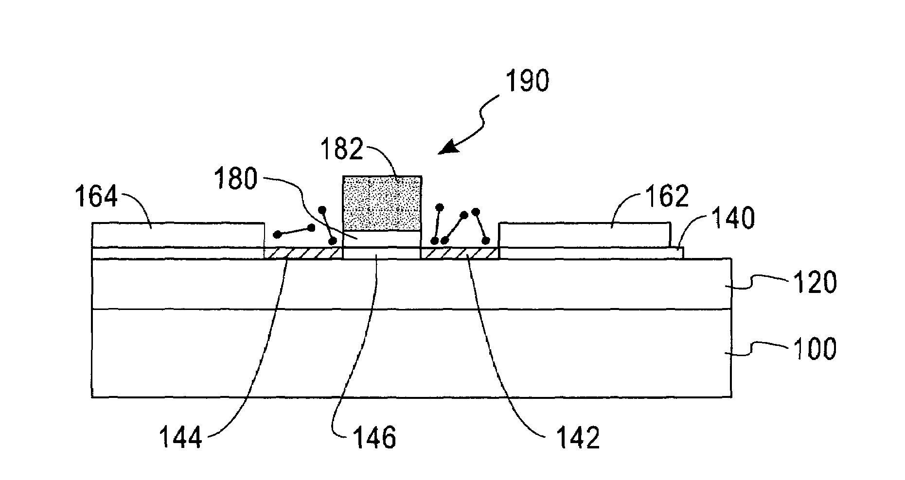
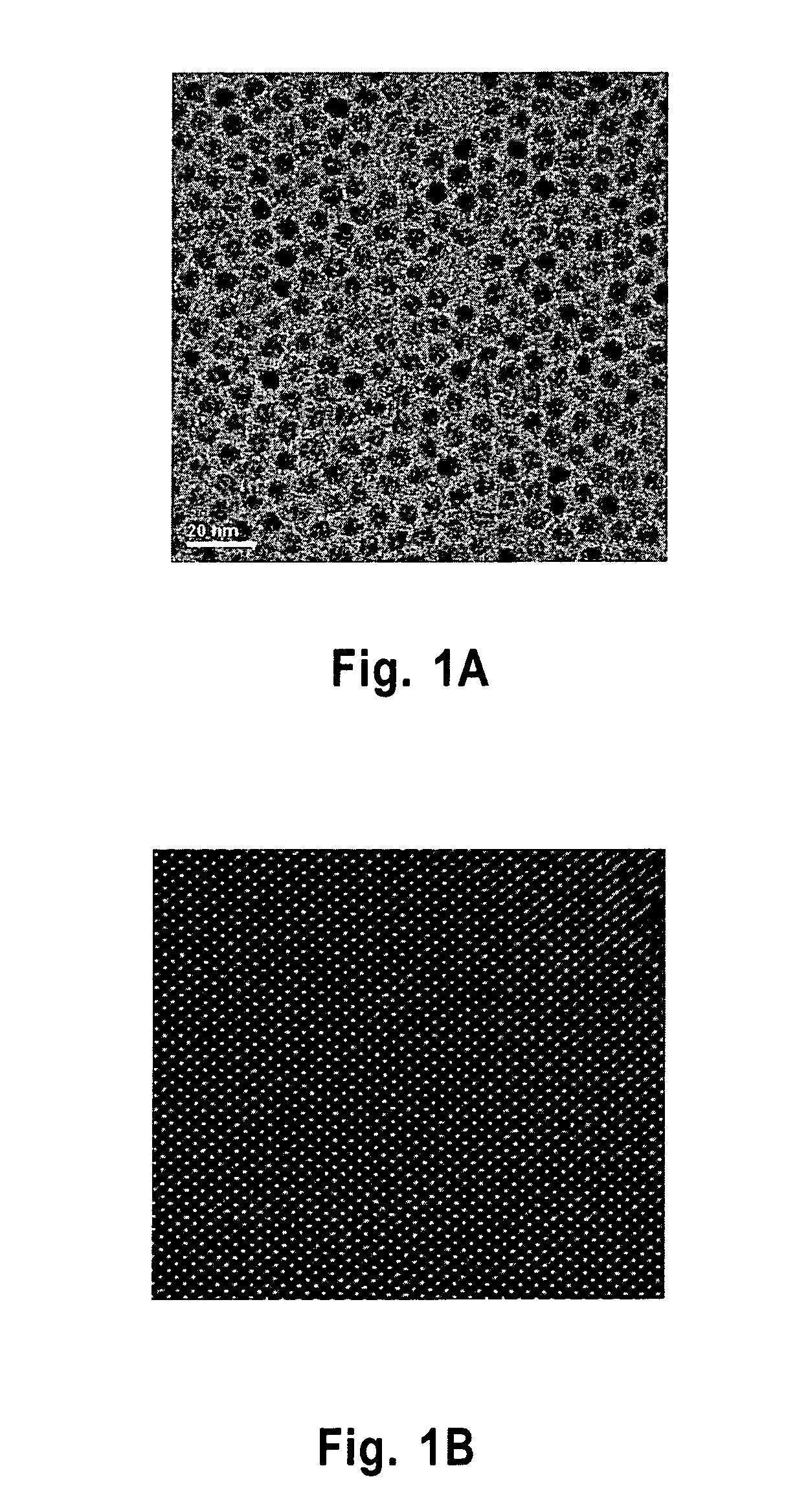
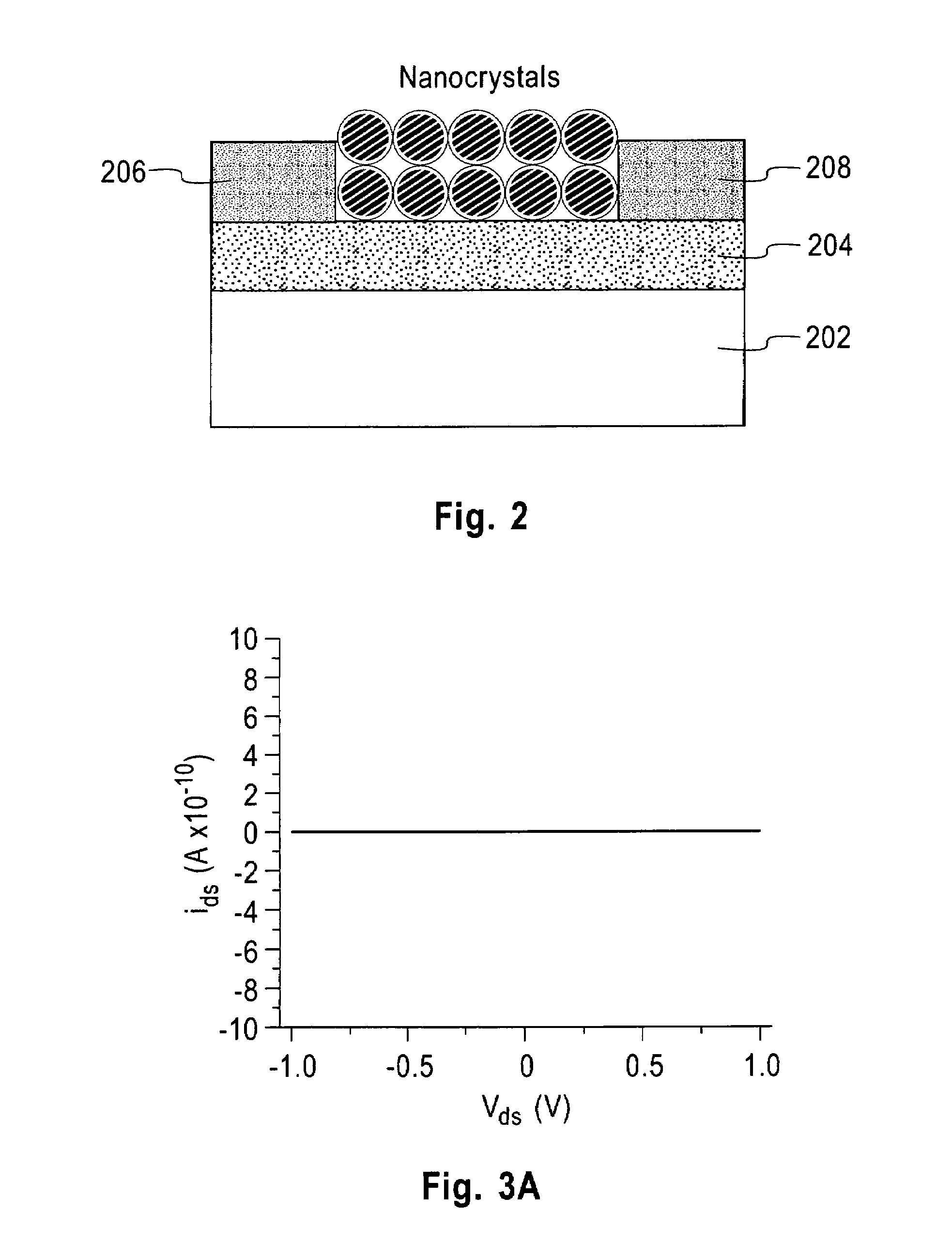
[0031]One aspect of the present invention relates to a method of forming a FET having a semiconductor nano-component (or nano-structure) that has been doped by exposing the nano-component to a suitable organic amine-containing dopant. The nano-component includes nanotubes, nanocrystals and nanowires comprising one or more semiconductor material containing an element from Groups III, IV, V and VI of the Periodic Table; e.g., Si, Ge, Sn, Se, Te, B, P, As, Sb, Bi, AlN, AlP, AlAs, AlSb, GaAs, GaP, GaSb, InN, InP, InAs, InSb, In2O3, In2S3, In2Se3, In2Te3, CdS, CdSe, CdTe, ZnO, ZnS, ZnSe, ZnTe, SnO, SnS, SnSe, SnTe, HgS, HgSe, HgTe, GeS, GeSe, GeTe, PbO, PbS, PbSe, PbTe, Sb2S3, Sb2Se3, Sb2Te3 and appropriate combinations thereof. Another aspect of the invention provides a device comprising a semiconductor nano-component such as PbSe. As used herein, a nano-component refers to a component having its smallest dimension being less than about 100 nm.

[0032]According to embodiments of this inve...


PUM

PropertyMeasurementUnit
temperatureaaaaaaaaaa

Abstract

A device comprising a doped semiconductor nano-component and a method of forming the device are disclosed. The nano-component is one of a nanotube, nanowire or a nanocrystal film, which may be doped by exposure to an organic amine-containing dopant. Illustrative examples are given for field effect transistors with channels comprising a lead selenide nanowire or nanocrystal film and methods of forming these devices.

Description

CROSS REFERENCE TO RELATED APPLICATIONS[0001]This application claims priority to U.S. Provisional Appln. 60 / 629,100, “Device Comprising Doped Nano-Component and Method of Forming the Device”, filed on Nov. 18, 2004; which is incorporated herein by reference in its entirety. This application also contains subject matter related to U.S. application Ser. No. 10 / 991,582, “Chemical Doping of Nano-Components”, filed on Nov. 18, 2004.FIELD OF THE INVENTION[0002]The invention relates to a device comprising a doped nano-component and a method of forming the device.BACKGROUND OF THE INVENTION[0003]Semiconductor nanocrystals constitute a novel class of materials with physical properties that are significantly different from those of bulk materials. The electronic structure of semiconductor nanocrystals is strongly dependent on the nanocrystal size and shape providing additional options to design and optimize material properties [Murray et al., Ann. Rev. Mater. Sci., 30, 542 (2000)]. Moreover, ...

Claims


Application Information

Patent Timeline
Patent Type & Authority Patents(United States)
IPC IPC(8): H01L21/336
CPCB82Y10/00B82Y20/00B82Y30/00H01L29/04H01L29/0673H01L29/7869H01L29/78696H01L51/0049H01L51/0545H01L29/78684H01L2251/5369Y10S977/938H10K85/225H10K10/466H10K2102/331
Inventor AFZALI-ARDAKANI, ALIKAGAN, CHERIE R.MURRAY, CHRISTOPHER B.SANDSTROM, ROBERT L.TALAPIN, DMITRI V.
Owner GLOBALFOUNDRIES INC
Why Eureka
Try Eureka