Analog-to-digital converter with noise compensation in CMOS image sensor

a technology of analog-to-digital converter and image sensor, which is applied in the field of analog-to-digital converter in cmos (complementary metal oxide semiconductor) image sensor, can solve the problems of cmos image sensor being generally inferior to cmos image sensor in electro-optical characteristics, disadvantageous driving mechanism of ccd image sensor for continuous transfer of charge carriers,

Inactive Publication Date: 2008-08-05
SAMSUNG ELECTRONICS CO LTD
View PDF4 Cites 17 Cited by
  • Summary
  • Abstract
  • Description
  • Claims
  • Application Information

AI Technical Summary

Benefits of technology

[0010]Accordingly, embodiments of the present invention provide cancellation of power noise in the trip point voltage for a singled-ended inverting amplifier in an analog-to-digital converter.

Problems solved by technology

However, the CCD image sensor disadvantageously has a complicated driving mechanism for continuous transfer of charge carriers.
Additionally, the CCD image sensor consumes relatively high power.
The CMOS image sensor is generally inferior to the CCD image sensor in electro-optical characteristics.
However, the CMOS image sensor has lower power consumption and higher integration density than the CCD image sensor.
However, the single-ended inverting amplifier has a trip point voltage that may be prone to power noise.
Such noise for the trip point voltage causes image distortion.

Method used


Image

  • Analog-to-digital converter with noise compensation in CMOS image sensor
  • Analog-to-digital converter with noise compensation in CMOS image sensor
  • Analog-to-digital converter with noise compensation in CMOS image sensor

Examples


Embodiment Construction

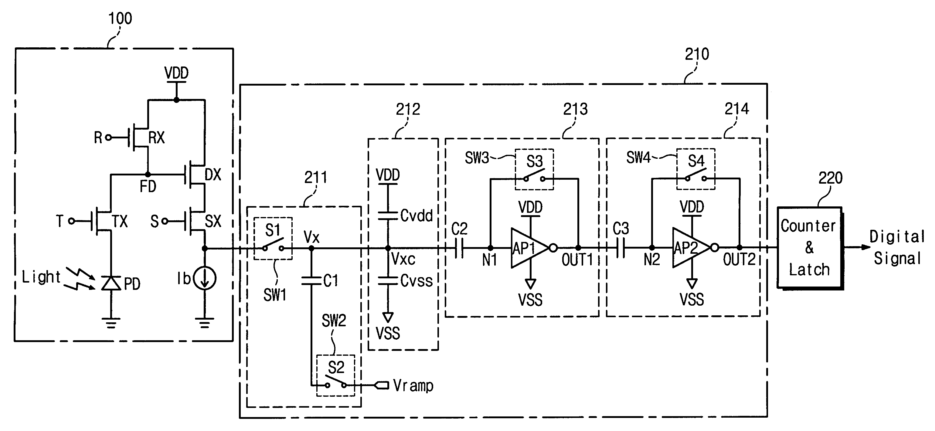
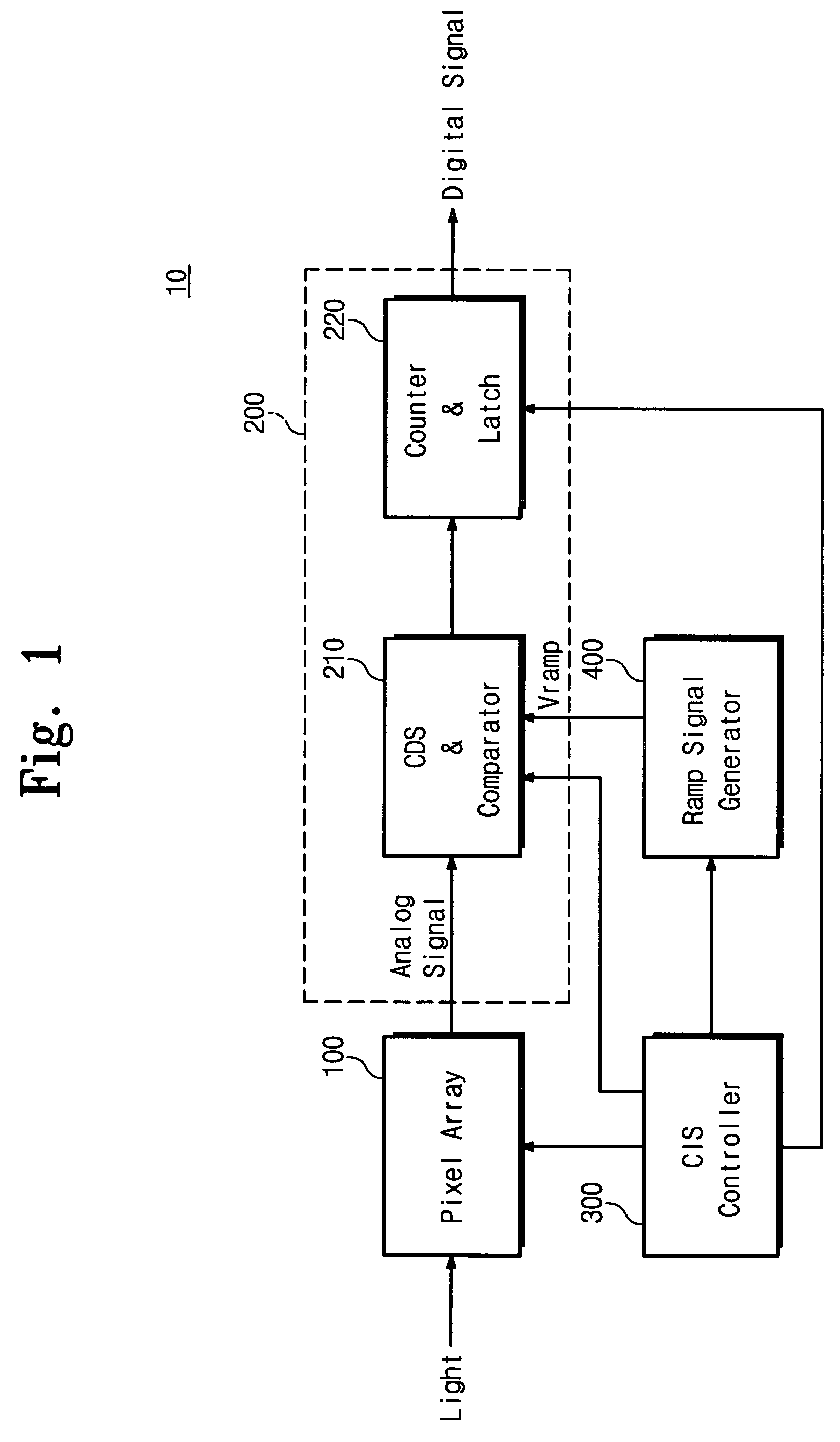
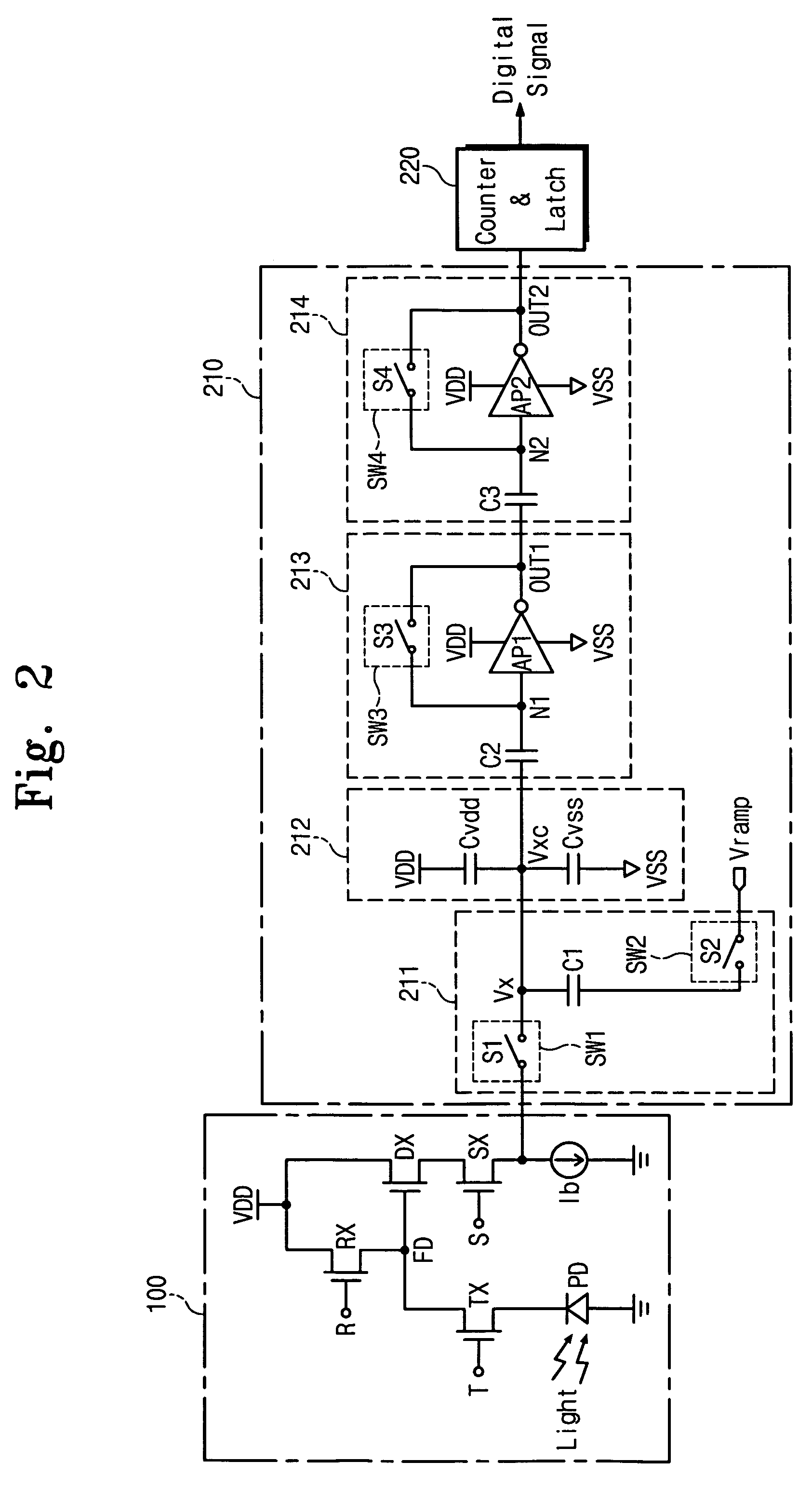
[0026]FIG. 1 is a block diagram of a CMOS (complementary metal oxide semiconductor) image sensor 10 according to an embodiment of the present invention. The CMOS image sensor (CIS) 10 includes a pixel array 100, a correlated double-sampling (CDS) ADC (analog-to-digital converter) 200, a CIS controller 300, and a ramp signal generator 400.

[0027]The pixel array 100 is comprised of a plurality of unit pixel circuits that generate electric signals from an image. Each unit pixel circuit includes a photodiode for transforming incident light for such an image into an analog image signal and for outputting such an image signal. The CDS ADC 200 includes a CDS (correlated double sampling) and comparator unit 210 and a conversion unit 220 that is implemented with a counter and a latch in one embodiment of the present invention. The CDS ADC 200 also includes a CIS controller 300 and a ramp signal generator 400.

[0028]The CIS controller 300 generates control signals, R, T, and S for operating the...


PUM


Abstract

An analog-to-digital converter includes an amplifying unit and a noise compensation unit. The amplifying unit amplifies a difference between a trip point voltage and a modified signal voltage. The trip point voltage has a first power noise component, and the noise compensation unit incorporates a second power noise component into an original signal voltage to generate the modified signal voltage. Thus, the power noise components are cancelled in the difference.

Description

BACKGROUND OF THE INVENTION[0001]This application claims priority to Korean Patent Application No. 2005-71139, filed on Aug. 3, 2005 in the Korean Intellectual Property Office, the disclosure of which is incorporated herein in its entirety by reference.[0002]1. Field of the Invention[0003]The present invention relates generally to analog-to-digital conversion in CMOS (complementary metal oxide semiconductor) image sensors, and more particularly, to compensating for power noise during such analog-to-digital conversion.[0004]2. Description of the Related Art[0005]An Image sensor converts an image into electrical signals using photo-conversion. An image sensor is generally classified into either a charge-coupled device (CCD) type or a complementary metal-oxide-semiconductor (CMOS) image sensor (CIS) type depending on the mechanism for generating and transferring charge carriers.[0006]The CCD image sensor transfers electrons generated from incident light to an output port using gate pul...

Claims


Application Information

Patent Timeline
Patent Type & Authority Patents(United States)
IPC IPC(8): H01L27/00H01J40/14
CPCH03M1/0845H04N5/378H04N5/3575H03M1/56H04N25/616H04N25/75H04N25/60H04N25/77
Inventor LEE, MYOUNG-SU
Owner SAMSUNG ELECTRONICS CO LTD
Why Eureka
Try Eureka