Metal-insulator transition switching transistor and method for manufacturing the same

a transition switching transistor and metal-insulator technology, applied in transistors, electrical devices, semiconductor devices, etc., can solve the problems of low current gain, difficult cooling (or emission) of heat induced by joule heating in the metal state, and defects of high-speed switching transistors. , to achieve the effect of stable thermally, high current gain characteristic, and small siz

Inactive Publication Date: 2008-08-05
ELECTRONICS & TELECOMM RES INST
View PDF6 Cites 21 Cited by
  • Summary
  • Abstract
  • Description
  • Claims
  • Application Information

AI Technical Summary

Benefits of technology

[0007]The present invention is directed to a metal-insulator-transition switching transistor having a small size and high current gain characteristic, and a method for manufacturing the same. In addition, a transistor of the present invention is stable thermally.

Problems solved by technology

However, there has been a problem that a current gain decreases due to an increase of a depletion area in the channel when a channel length in the channel layer is reduced, since the two kinds of transistors use a semiconducting regime as a current channel layer.
In the structure, cooling (or emission) of heat induced by Joule heating in the metal state is not easy.
These are defects for a high speed switching transistor.

Method used


Image

  • Metal-insulator transition switching transistor and method for manufacturing the same
  • Metal-insulator transition switching transistor and method for manufacturing the same
  • Metal-insulator transition switching transistor and method for manufacturing the same

Examples


Embodiment Construction

[0018]The present invention will be described in detail by way of a preferred embodiment with reference to accompanying drawings, in which like reference numerals are used to identify the same or similar parts.

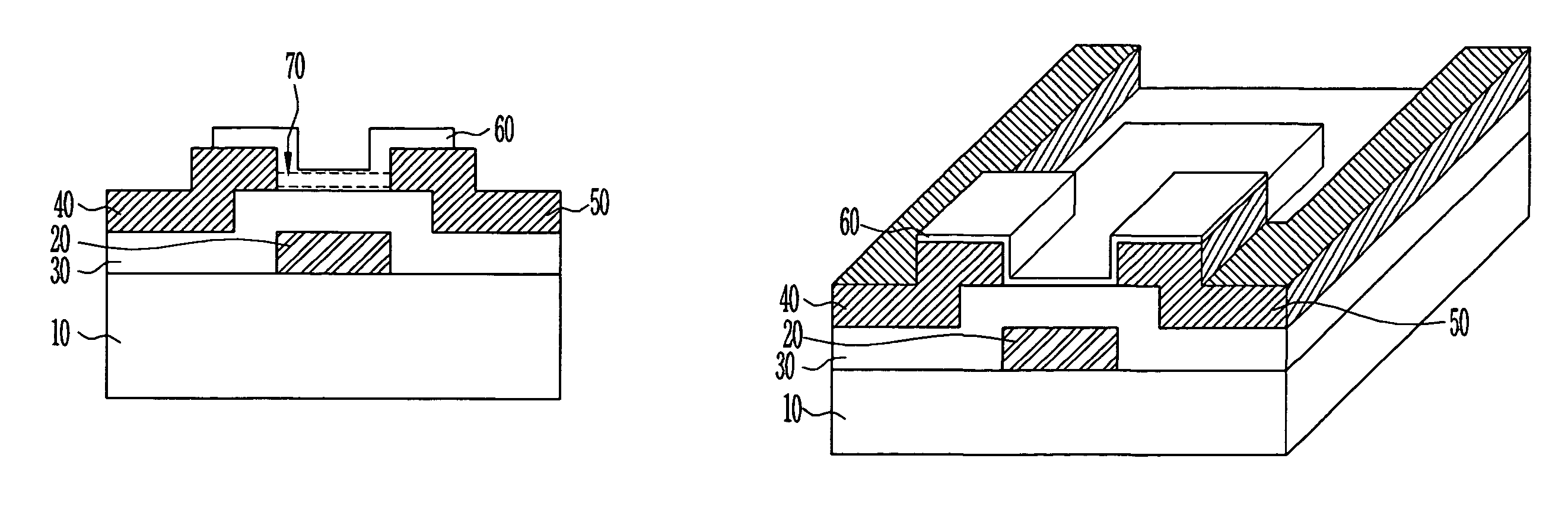
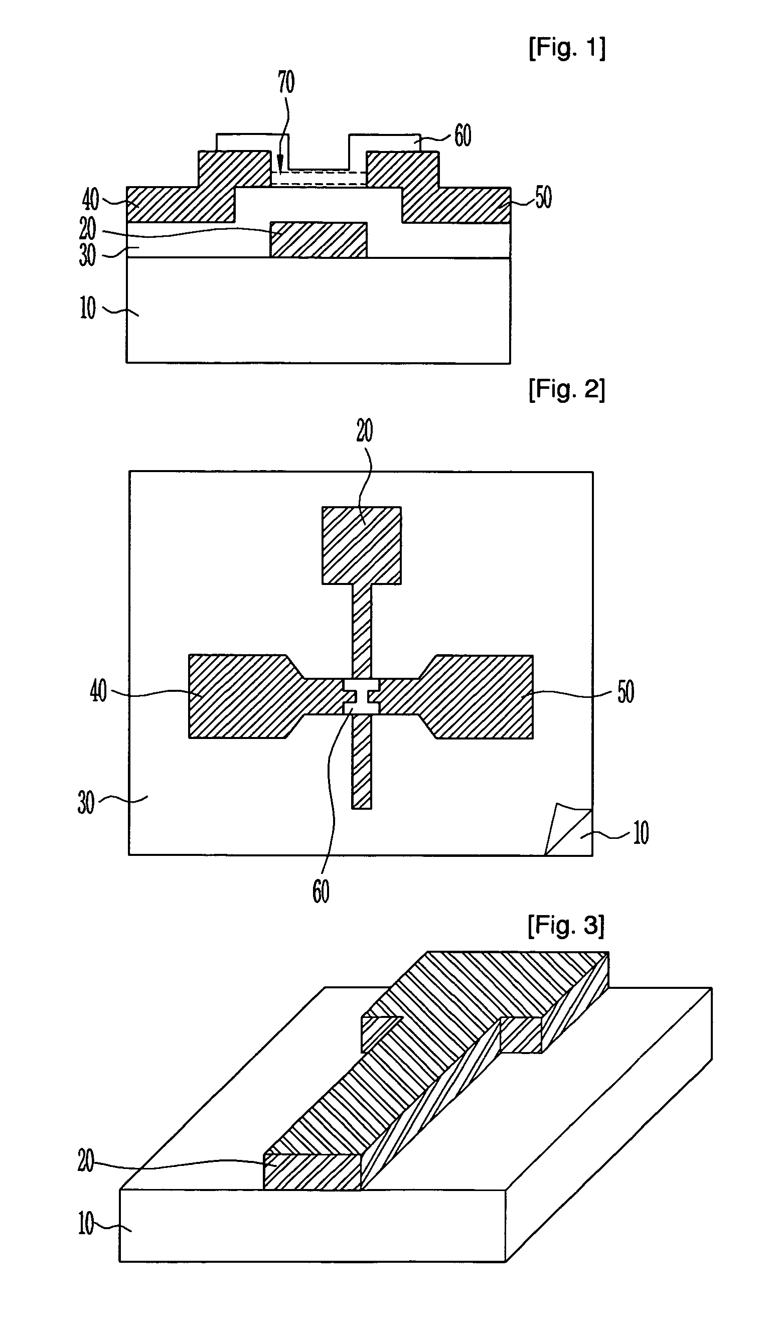
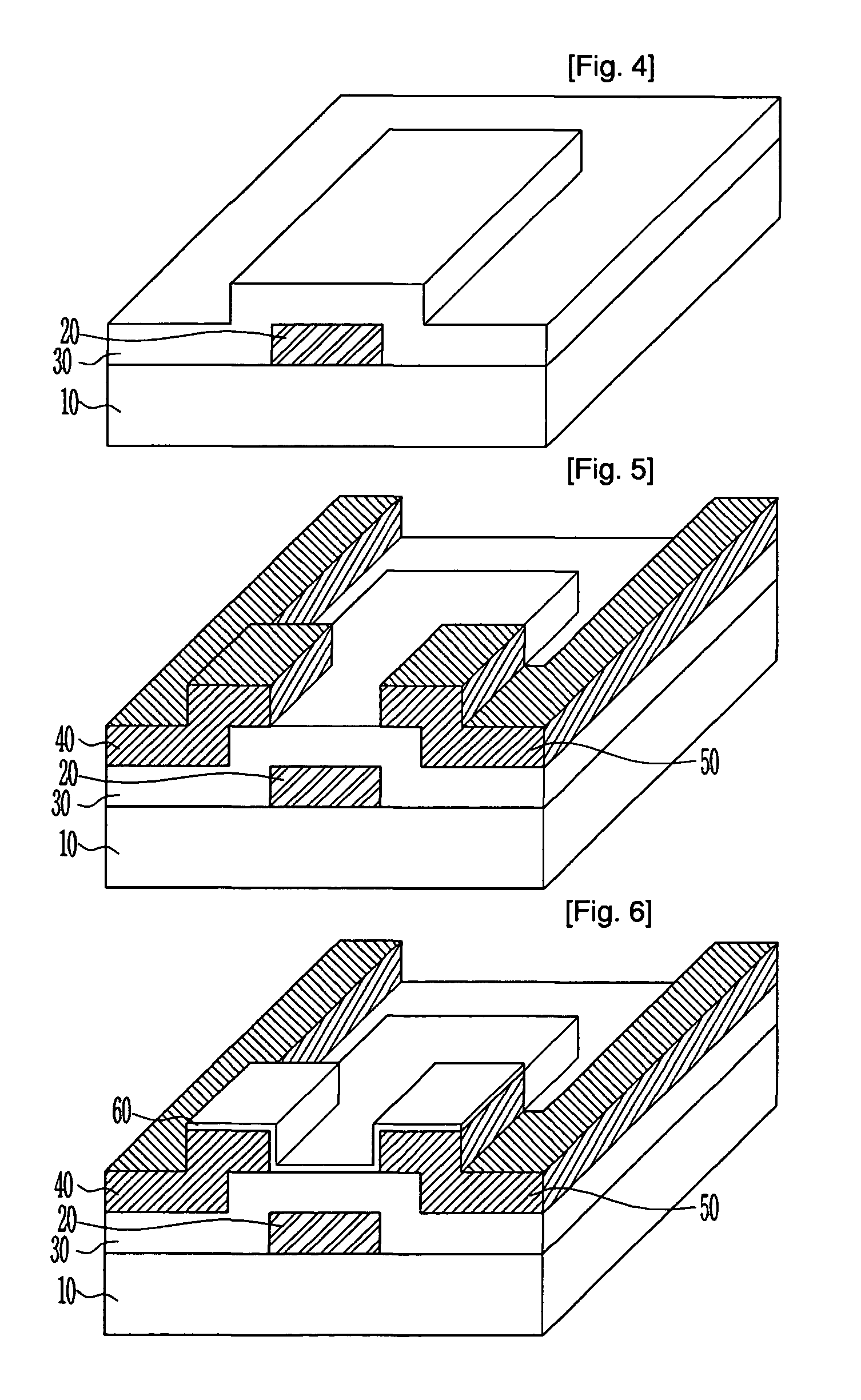
[0019]FIGS. 1 and 2 are a cross sectional view and a plane view of a metal-insulator-transition (MIT) switching transistor according to a preferred embodiment of the present invention.

[0020]Referring to FIGS. 1 and 2, a metal-insulator-transition transistor comprises a substrate 10, a gate electrode 20, a gate insulation film 30, a source electrode 40, a drain electrode 50, and a metal-insulator-transition channel layer 60.

[0021]Preferably, the substrate 10 is a silicon substrate having an excellent thermal conductivity. In case where a vanadium dioxide (VO2) thin film having a thermally unstable characteristic is used for the metal-insulator-transition channel layer 60, it is possible to prevent that a transistor characteristic becomes deteriorated due to a heat, which is gen...


PUM


Abstract

Provided is a metal-insulator-transition switching transistor with a gate electrode on a silicon substrate (back-gate structure) and a metal-insulator-transition channel layer of VO2 that changes from an insulator phase to a metal phase, or vice versa, depending on a variation of an electric field, and a method for manufacturing the same, whereby it is possible to fabricate a metal-insulator-transition switching transistor having high current gain characteristics and being stable thermally.

Description

BACKGROUND[0001]1. Field of the Invention[0002]The present invention relates to a metal-insulator transition switching transistor (three terminal device) and a method for manufacturing the same and, more particularly, to a metal-insulator-transition switching transistor using a vanadium dioxide (VO2) thin film as a metal-insulator-transition channel layer, and a method for manufacturing the same.[0003]2. Discussion of Related Art[0004]As a conventional transistor that has been developed for the purpose of an ultra small size and an ultra high speed, there are metal-oxide-semiconductor field-effect transistor (MOSFET) and Mott transistor developed by IBM, representatively. The Mott transistor has been disclosed in “D. M. Newns, J. A. Misewich, C. C. Tsuei, A. Gupta, B. A. Scott, and A. Schrott, Appl. Phys. Lett. Vol. 73, 780 (1998)”. However, there has been a problem that a current gain decreases due to an increase of a depletion area in the channel when a channel length in the chann...

Claims


Application Information

Patent Timeline
Patent Type & Authority Patents(United States)
IPC IPC(8): H01L29/772H01L29/78H01L49/00
CPCH01L49/003H10N99/03H01L29/78
Inventor YOON, DOO HYEBKIM, HYUN TAKCHAE, BYUNG GYUKANG, KWANG YONGMAENG, SUNG LYUL
Owner ELECTRONICS & TELECOMM RES INST
Why Eureka
Try Eureka