Method for the heat treatment of substrates

a substrate and heat treatment technology, applied in the field of semiconductor processing, can solve the problems of reducing the heat-up rate, reducing the heat-transmission rate, so as to reduce the heat-transmission rate

Inactive Publication Date: 2008-08-12
ASM INTERNATIONAL
View PDF53 Cites 46 Cited by
  • Summary
  • Abstract
  • Description
  • Claims
  • Application Information

AI Technical Summary

Problems solved by technology

The small gap results in a particularly rapid heat transfer from the heated blocks to the wafer by conduction through the gas.
In comparison, where a transport arm transports a substrate into the reactor and then continues to support the substrate during processing, mechanical contact during processing by support fingers of a transport arm results in cold spots on the wafer during heat-up at the contact positions with the support fingers, as the support fingers represent extra thermal mass that needs to be heated and that locally slows down the heat-up rate.
Alternatively, where a substrate is transported to the reactor and then handed off to support pins that remain in the reactor after processing, mechanical contact during processing by those support pins results in hot spots on the wafer at the contact positions when the wafer is handed-off and contacts the support pins.
However, changing the temperature of reactors such as the Levitor® reactor, and cooling-down the reactor, in particular, is a very time-consuming process that can negatively influence the applicability of such a reactor for performing sequences of processes requiring different process temperatures.

Method used


Image

  • Method for the heat treatment of substrates
  • Method for the heat treatment of substrates
  • Method for the heat treatment of substrates

Examples


example

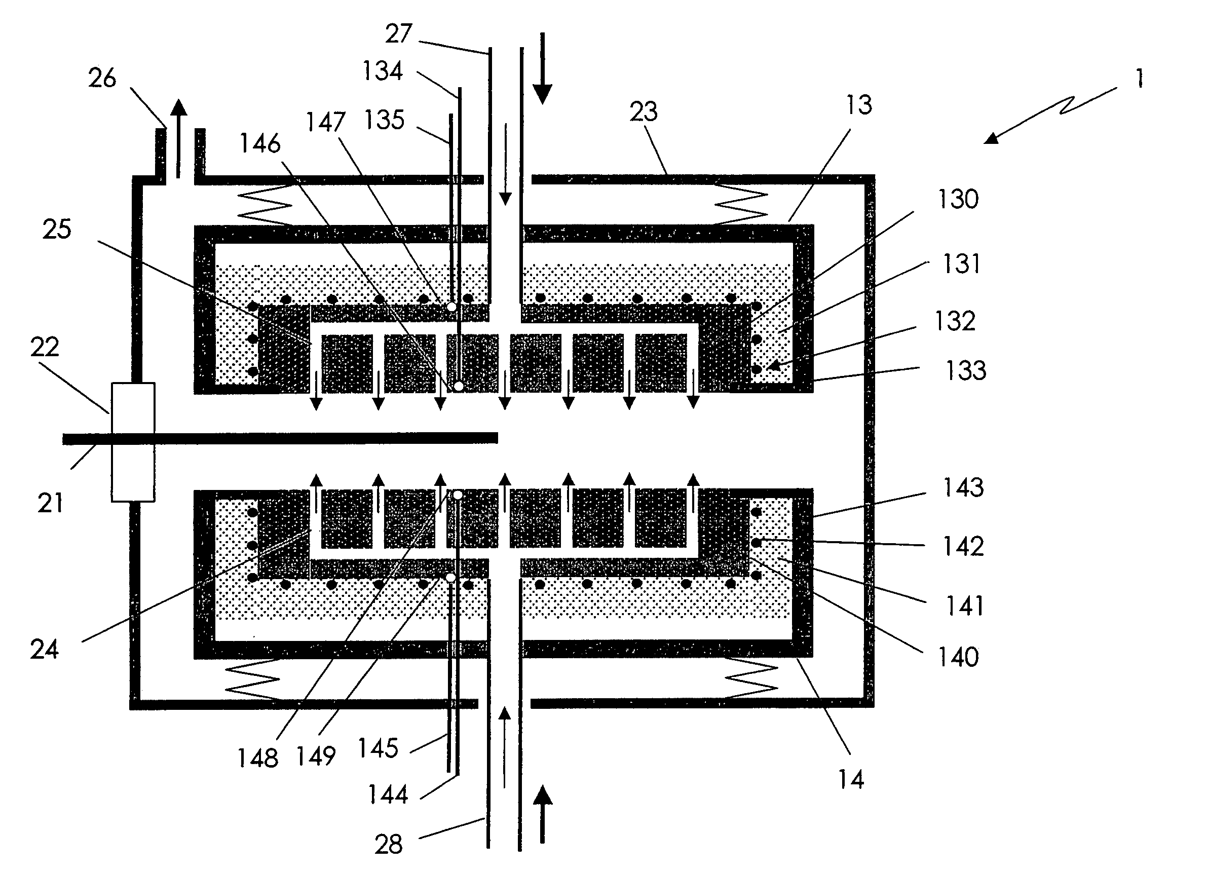
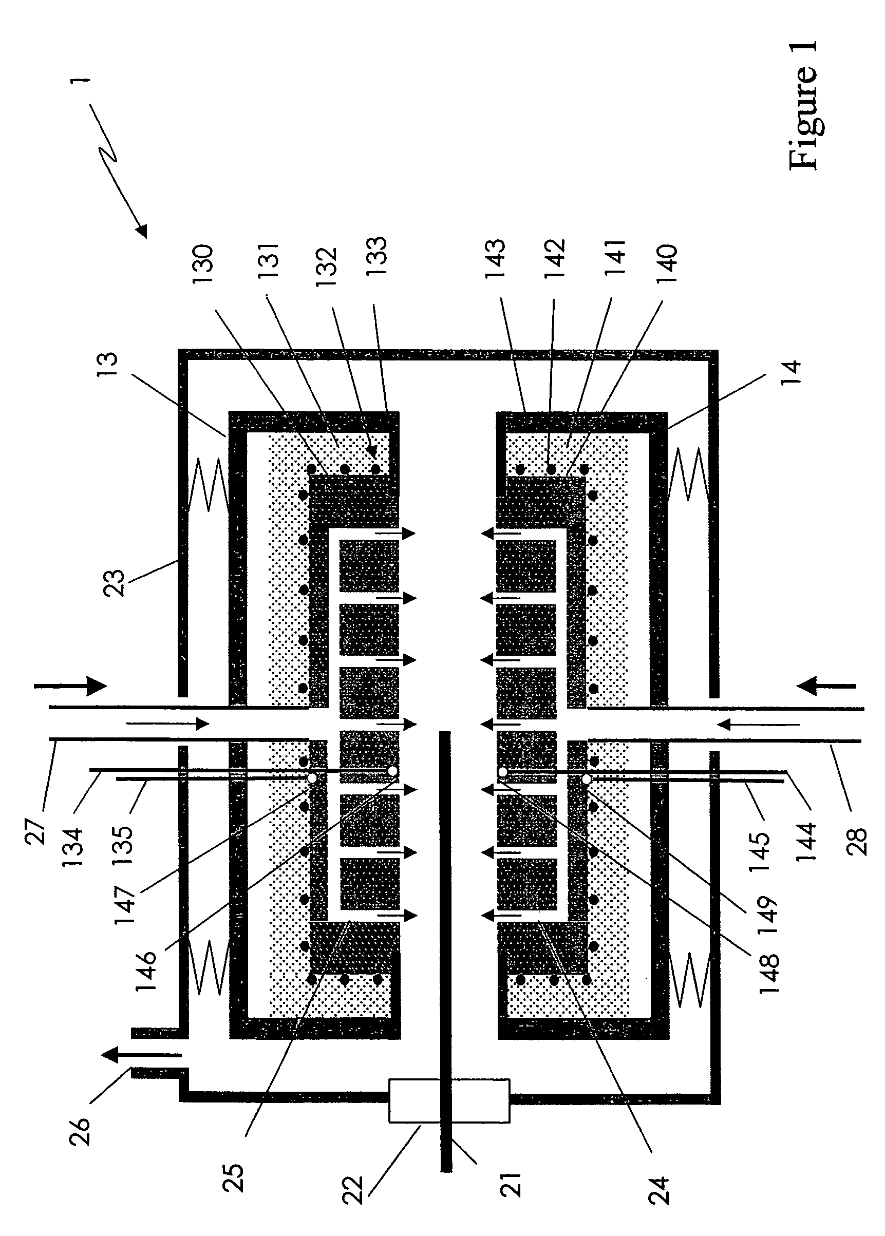
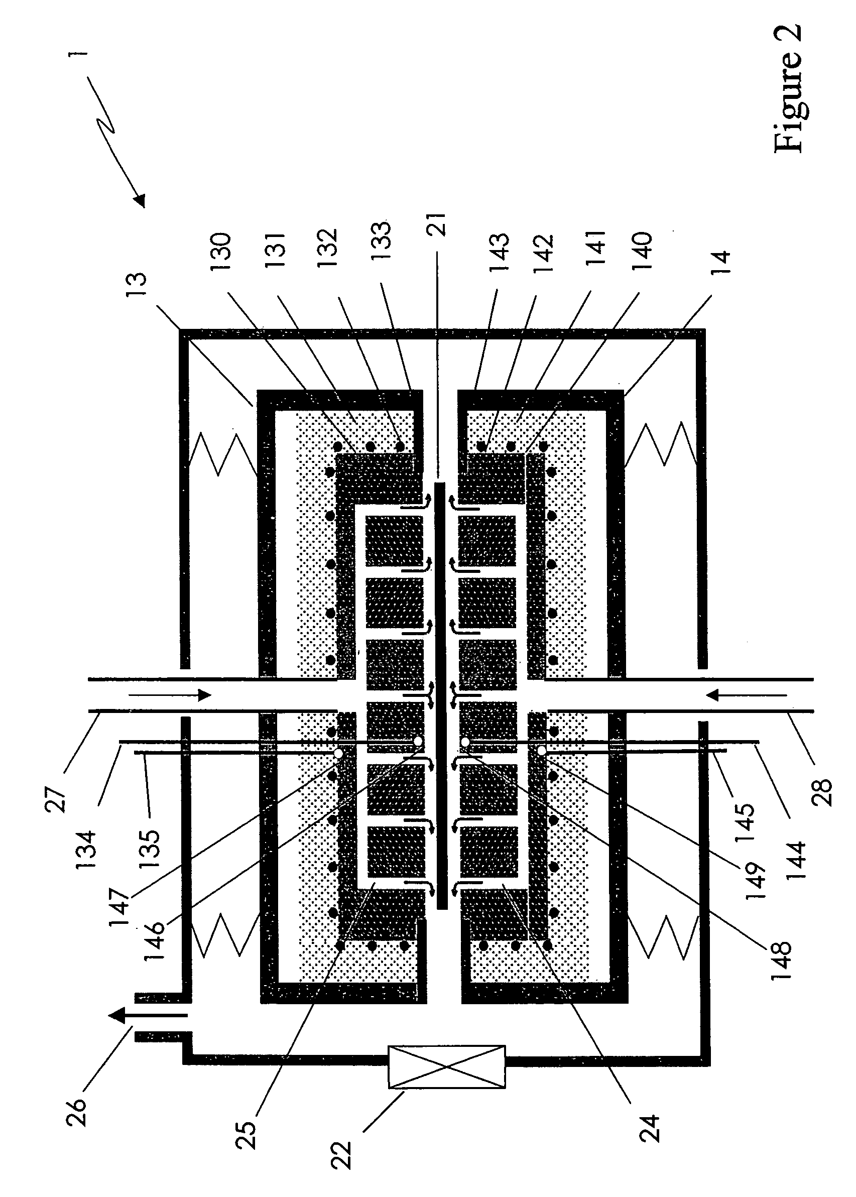
[0055]A silicidation process involving two anneals was carried out. The first anneal of these two anneals was carried out according to either a conventional anneal or to an anneal according to the methods described herein and the results for these two anneals were compared.

[0056]In the conventional first anneal, silicon wafers having a nickel (Ni) film on their top surface received an anneal in a Levitor® reactor, commercially available from ASM International, N.V. of Bilthoven, The Netherlands, with the reactor blocks and furnace bodies at a constant temperature of 350° C. The blocks remained in the closed position, with the wafer at a distance of 0.15 mm from each of the reactor blocks, for 18 seconds.

[0057]In the first anneal according to the methods described herein, similar silicon wafers received an anneal in the Levitor® reactor with the reactor blocks and furnace bodies set at a temperature of 450° C. After introducing the wafer into the reactor, the blocks remained in the c...


PUM

PropertyMeasurementUnit
temperaturesaaaaaaaaaa
temperatureaaaaaaaaaa
distanceaaaaaaaaaa

Abstract

A substrate undergoes a semiconductor fabrication process at different temperatures in a reactor without changing the temperature of the reactor. The substrate is held suspended by flowing gas between two heated surfaces of the reactor. Moving the two heated surfaces in close proximity with the substrate for a particular time duration heats the substrate to a desired temperature. The desired temperature is then maintained by distancing the heated surfaces from the substrate and holding the heated surface at the increased distance to minimize further substrate heating.

Description

REFERENCE TO RELATED APPLICATIONS[0001]This application is a continuation-in-part of U.S. patent application Ser. No. 10 / 700,298, filed Oct. 31, 2003 now U.S. Pat. No. 7,022,627.[0002]In addition, this application is related to U.S. application Ser. No. 10 / 151,207, METHOD AND DEVICE FOR THE HEAT TREATMENT OF SUBSTRATES, filed May 16, 2002; U.S. application Ser. No. 10 / 186,269, METHOD AND APPARATUS FOR THE TREATMENT OF SUBSTRATES, filed Jun. 27, 2002; U.S. application Ser. No. 10 / 141,517, TEMPERATURE CONTROL FOR SINGLE SUBSTRATE SEMICONDUCTOR PROCESSING REACTOR, filed May 8, 2002; and U.S. application Ser. No. 10 / 410,699, TEMPERATURE CONTROL FOR SINGLE SUBSTRATE SEMICONDUCTOR PROCESSING REACTOR, filed Apr. 8, 2003.BACKGROUND OF THE INVENTION[0003]1. Field of the Invention[0004]This invention relates generally to semiconductor processing and, more particularly, to the heat treatment of substrates, including semiconductor wafers or flat panel displays.[0005]2. Description of the Relate...

Claims


Application Information

Patent Timeline
Patent Type & Authority Patents(United States)
IPC IPC(8): H01L21/02H01L21/00H01L21/26H01L21/324H01L21/42H01L21/477H01L21/683
CPCH01L21/324H01L21/6838H01L21/67109H01L21/42H01L21/477H01L21/67248H01L21/67784
Inventor GRANNEMAN, ERNST H. A.KUZNETSOV, VLADIMIR I.PAGES, XAVIERVERMONT, PASCAL G.TERHORST, HERBERTSNIJDERS, GERT-JAN
Owner ASM INTERNATIONAL
Why Eureka
Try Eureka