Low-loss integrated waveguide feed for wafer-scale heterogeneous layered active electronically scanned array

a technology of electronic scanning arrays and waveguides, applied in the field of phased array antennas, antennas, instruments, etc., can solve the problems of large losses at the subarray level, and achieve the effects of reducing the number of interconnection line requirements, reducing cost, and increasing performan

Active Publication Date: 2008-08-12
ROCKWELL COLLINS INC
View PDF3 Cites 20 Cited by
  • Summary
  • Abstract
  • Description
  • Claims
  • Application Information

AI Technical Summary

Benefits of technology

[0017]It is an advantage of the present invention to utilize wafer-scale integration to reduce cost and increase performance.
[0018]It is an advantage of the present invention to reduce the number of interconnection line requirements in an electrically large ESA.
[0019]It is a feature of the present invention to reduce losses in a wafer-scale ESA.
[0020]It is a feature of the present invention to provide a low-cost wafer-scale ESA with simple construction.

Problems solved by technology

One of the major challenges in ESA design is to provide cost effective antenna array phase shifting methods and techniques along with dual-band operation of the ESA.
One of the problems with the coplanar waveguides and microstrip feed implementations at the subarray level are the large losses.

Method used


Image

  • Low-loss integrated waveguide feed for wafer-scale heterogeneous layered active electronically scanned array
  • Low-loss integrated waveguide feed for wafer-scale heterogeneous layered active electronically scanned array
  • Low-loss integrated waveguide feed for wafer-scale heterogeneous layered active electronically scanned array

Examples


Embodiment Construction

[0031]The present invention is for a wafer-scale heterogeneous layered active electronically scanned array (ESA) with a low-loss integrated waveguide feed.

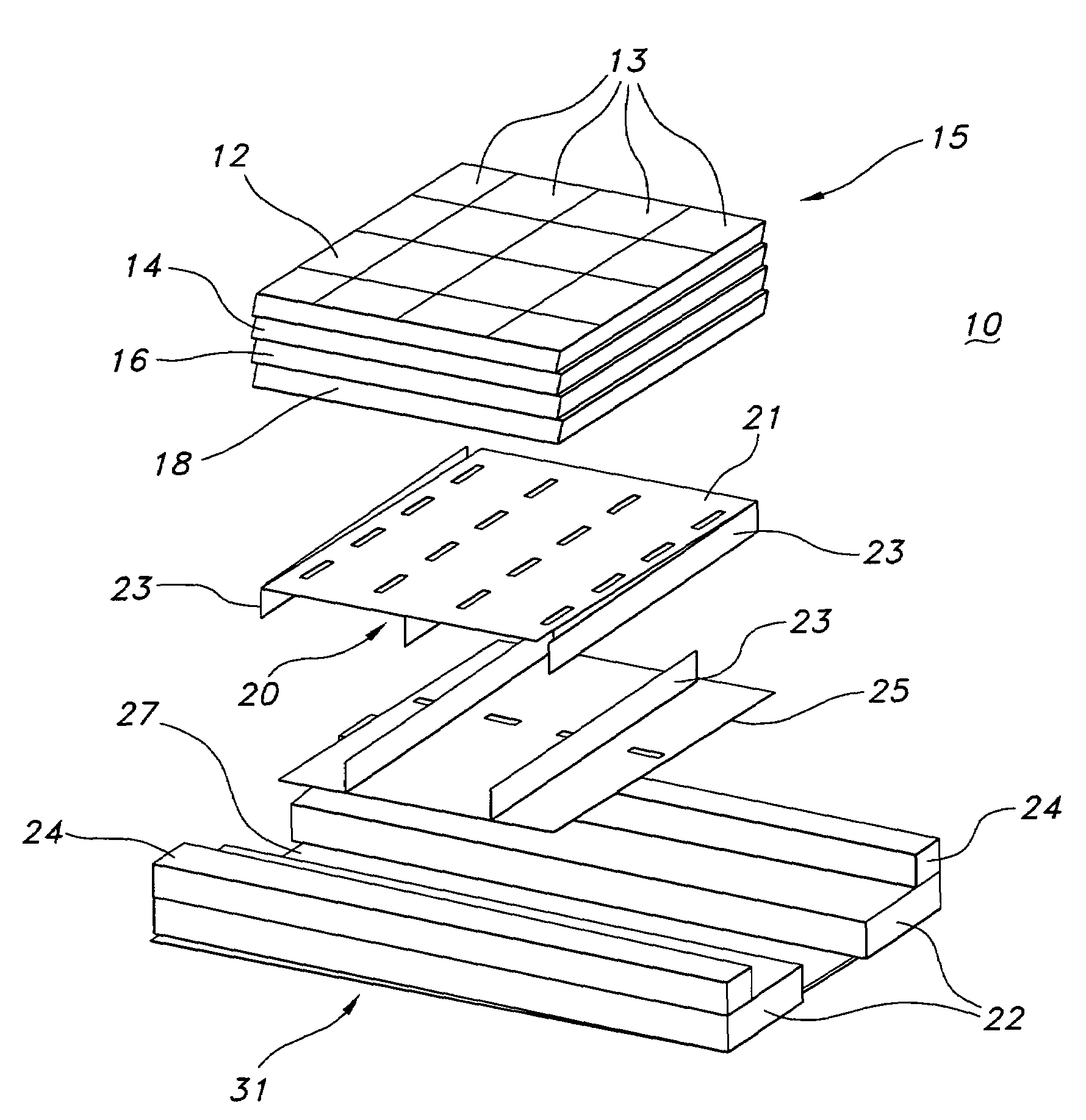
[0032]FIG. 1 shows a portion of a wafer-scale heterogeneous layered active electronically scanned array (ESA) 10 with a wafer-scale subarray module 15 that is fed by a waveguide subarray combiner 20. The wafer-scale subarray module 15 is a stand-alone integrated multilayer m×m or m×n stack of transmit / receive (T / R) modules 13 vertically oriented within a cell with λ / 2×λ / 2 spacing. The λ / 2×λ / 2 (free space) spacing is crucial to prevent grating lobes. The waveguide subarray combiner 20 feeds each of the T / R modules 13 in the subarray module 15. The subarray module 15 in FIG. 1 is shown with 16 T / R modules in a 4×4 array. Larger or smaller arrays of T / R modules 13 may also be used.

[0033]The wafer-scale subarray module 15 may be made up of an antenna layer 12, a switch 2 layer 14, a power amplifier (PA) layer 16, and a switch 1 and a ...


PUM


Abstract

A wafer-scale heterogeneous layered active electronically scanned array (ESA) utilizes a low-loss integrated waveguide feed. The ESA is formed from wafer-scale subarray modules each of which comprises a multilayer stack to form transmit / receive (T / R) modules. Waveguide subarray combiners feed the T / R modules. A subarray combiner is a waveguide assembly bonded to a bottom layer in the multilayer stack. The bottom layer is a ground plane forming a top waveguide broadwall of the combiner. The waveguide subarray combiner may be formed from a variety of waveguide types and feeds the T / R modules using electric field probe coupling or an aperture slot coupling. A second layer feed structure forms the subarray modules into the ESA and feeds the waveguide subarray combiners. The second layer feed structure uses waveguides to feed the waveguide subarray combiners using E-field probes or aperture slot coupling on the bottom waveguide broadwall.

Description

BACKGROUND OF THE INVENTION[0001]This invention relates to antennas, phased array antennas, and specifically to a wafer-scale heterogeneous layered active electronically scanned array (ESA) with a low-loss, integrated waveguide feed.[0002]Electronically scanned arrays or phased array antennas offer significant system level performance enhancements for advanced communications, data link, radar, and SATCOM systems. The ability to rapidly scan the radiation pattern of the ESA allows the realization of multi-mode operation, LPI / LPD (low probability of intercept and detection), and A / J (antijam) capabilities. One of the major challenges in ESA design is to provide cost effective antenna array phase shifting methods and techniques along with dual-band operation of the ESA.[0003]It is well known within the art that the operation of a phased array is approximated to the first order as the product of the array factor and the radiation element pattern as shown in Equation 1 for a linear array...

Claims


Application Information

Patent Timeline
Patent Type & Authority Patents(United States)
IPC IPC(8): H01P5/12H01Q13/10H01Q3/00
CPCH01Q21/0093H01Q21/0006H01Q1/02G01S2013/0254
Inventor WEST, JAMES B.WILCOXON, ROSS K.
Owner ROCKWELL COLLINS INC
Why Eureka
Try Eureka