Light-emitting device
a technology of light-emitting devices and organic compounds, which is applied in the direction of discharge tube luminescence screens, natural mineral layered products, etc., can solve the problems of insufficient efficiency in these documents, insufficient synthesis of cooper coordination compounds, and poor luminescence efficiency of the devices, etc., to achieve high luminescence efficiency, low cost, and high stability
- Summary
- Abstract
- Description
- Claims
- Application Information
AI Technical Summary
Benefits of technology
Problems solved by technology
Method used
Image
Examples
examples 1 to 9
[0108]The following compounds were prepared according the reaction formulae (A) to (C), respectively. Also, the constructions of the respective compounds were identified through 1H-NMR (Bruker DPX-400NMR) and elemental analysis (Vario EL CHNOS). In the elemental analysis, the measured value of the element weight ratio of CHN was in good agreement to the calculated value of the element weight ratio of CHN within 0.5% or less error.
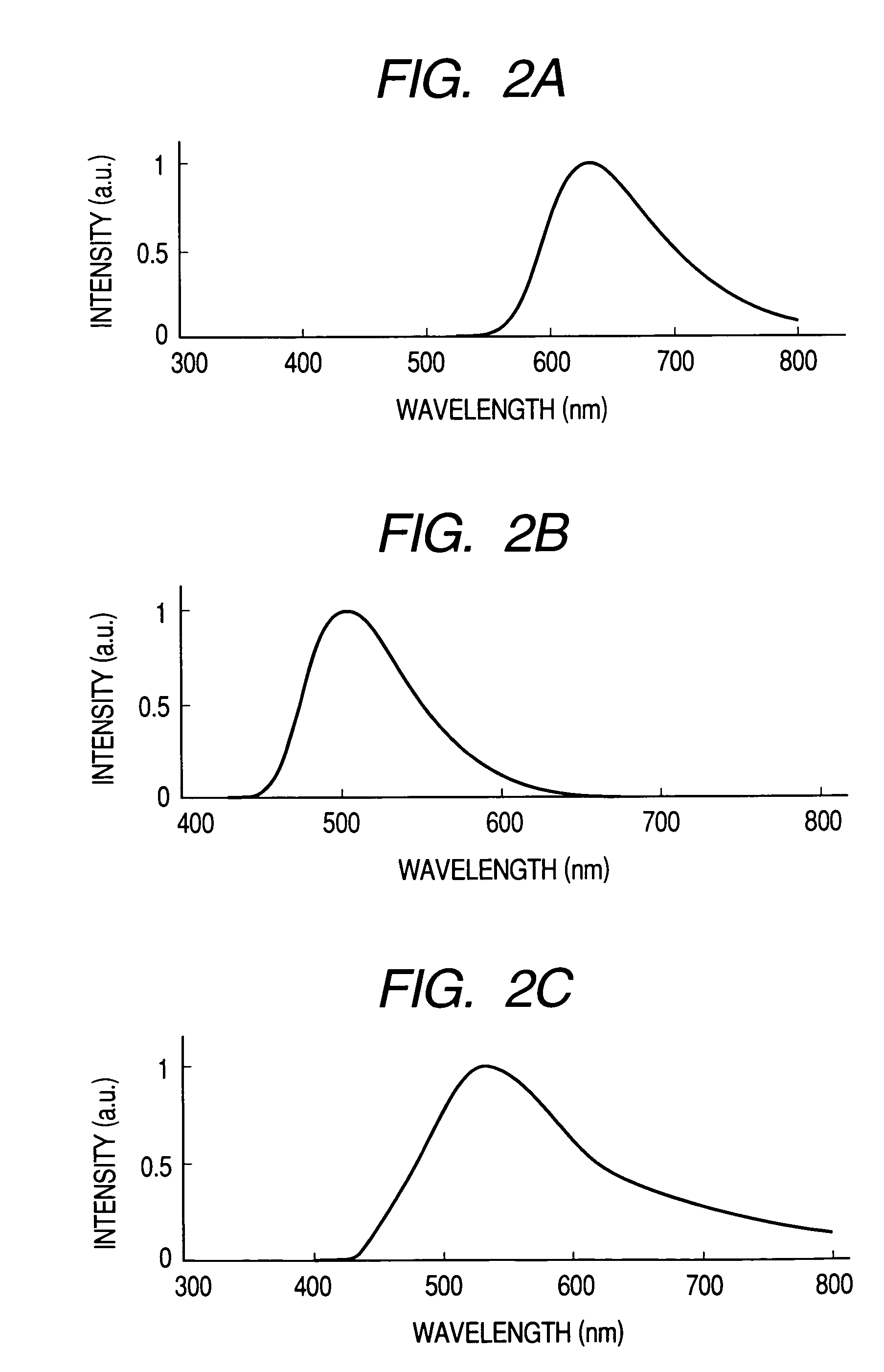
[0109]In addition, the luminescence property of each compound was measured by means of photoexcitation. Luminescence spectra were measured using F4500 manufactured by Hitachi Instruments Service Co., Ltd. (excitation wavelengths from 350 to 450 nm). All measurements were done in the solid powder state. Luminescent colors ranged from blue green to red. The results of the measurement on luminescence spectrum are listed in Table 5 below.
[0110]
TABLE 5LuminescenceExemplifiedwavelength ofExamplescompound No.solid powderHalf band width11001636 nm—21002632 nm109 nm...
examples 10 to 12
[0113]Organic EL devices were prepared using as light-emitting materials the exemplified compounds 1002, 1138, and 4005 synthesized in Examples 2, 4, and 8, respectively.
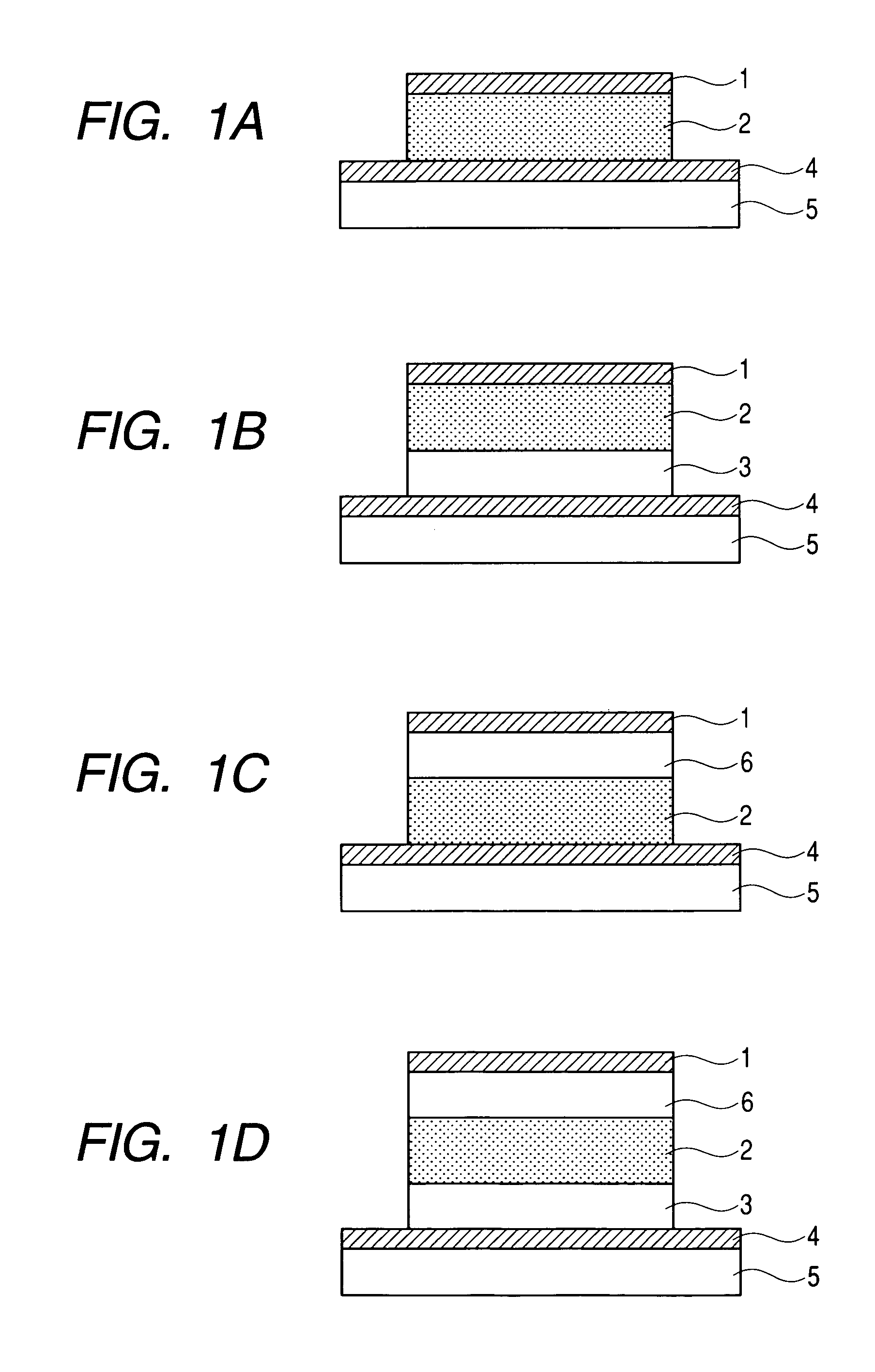
[0114]The configuration of a device having three organic layers shown in FIG. 1D was employed as a configuration of the organic EL device. More specifically, on a glass substrate (i.e., the transparent substrate 5), ITO (transparent electrode 4) of 100 nm in thickness was patterned so as to have an electrode area of 3.14 mm2.
[0115]On the ITO substrate, PEDOT (for organic EL) manufactured by Bayer AG was applied in 40 nm in film thickness by means of spin coating at a speed of 1,000 rpm (20 seconds). Then, the resulting coating was dried at 120° C. for 1 hour in a vacuum chamber. On the resulting layered product, subsequently, a solution, which contained 10 g of chlorobenzene, 92 mg of polyvinyl carbazole (an average molecular weight of 9,600), and 8 mg of the exemplified compound 1002, 1138, or 4005, was applied by ...
example 13
[0123]A light-emitting device was prepared by the same way as that of Example 12, except for a light-emitting layer. In this example, the light-emitting layer was prepared in a film thickness of 30 nm using 100% by mass of the exemplified compound 4005 by means of spin coating. For EL luminescence, good luminescence was observed at a luminescence of 200 cd / cm2 and good luminescence was retained even after 10 hours of current application. Therefore, it was found that the light-emitting device with higher luminescence efficiency than that of Example 12 can be attained by the formation of a light-emitting layer with 100% content of the exemplified compound 4005. The results are shown in Table 6.
PUM
| Property | Measurement | Unit |
|---|---|---|
| excitation wavelengths | aaaaa | aaaaa |
| area | aaaaa | aaaaa |
| thickness | aaaaa | aaaaa |
Abstract
Description
Claims
Application Information


