Display device

Inactive Publication Date: 2008-08-19
SHARP KK
View PDF7 Cites 2 Cited by
  • Summary
  • Abstract
  • Description
  • Claims
  • Application Information

AI Technical Summary

Benefits of technology

[0023]The present invention is made in view of the foregoing conventional problems, and an object is to provide a display device realizing desirable display quality by preventing influence of difference in leading manner of wiring and without increasing power consumption, even in an arrangement in which a plurality of signals related to each other, such as a clock signal of plural systems, are supplied to a driving circuit by using different wirings for the respective plural signals in order to simplify the structure of external interface, for example, in such a manner that a part of the signals is singly supplied, and the other part is supplied also to the other circuit.
[0027]In this case, to simplify the structure of an external interface, one clock signal is often supplied in parallel to the two data signal line driving circuits. However, in this case, there arises difference in wiring load between the first clock signal and the second clock signal in the data signal line driving circuit using two clock signal, i.e., the first clock signal (first signal) and the second clock signal (second signal) which is singly supplied, thus causing a problem of unevenness of signal delays. Such unevenness of signal delay changes phase relation between the first and second signal clocks from the optimal relation determined upon designing of the device. This change induces unevenness of sampling timing of image signals in the data signal line driving circuit, thus decreasing display quality.
[0030]With the foregoing arrangement, the wiring load of the first clock signal (first signal) supplied to both of the two data signal line driving circuits, and the wiring load of the second clock signal (second signal) singly supplied to one data signal line driving circuit can be adjusted to be even without the foregoing method of correcting the first and second signal clocks in an external circuit by using higher power consumption. Thus, it is possible to keep difference in delay time between the first and second clock signals within an allowable range. Consequently, sampling of image signal can be properly carried out in the data signal line driving circuit using both the first and second clock signals, thus improving display quality.
[0033]However, by thus providing the wiring load adjustment section for equalizing wiring load of the first clock signal (first signal) supplied to both of the two data signal line driving circuits, and wiring load of the second clock signal (second signal) singly supplied to one data signal line driving circuit, it is possible to suppress difference in signal delay between the first and second clock signals within an allowable range without the foregoing method of correcting the first and second signal clocks in an external circuit by using higher power consumption, so that the proper phase relation between the first and second clock signals can be maintained, thus maintaining desirable display quality.
[0034]More specifically, it is possible to provide a display device realizing desirable display quality by preventing influence of difference in leading manner of wiring and without increasing power consumption, even in an arrangement in which a plurality of signals related to each other, such as a clock signal of plural systems, are supplied to a driving circuit by using different wirings for the respective plural signals in order to simplify the structure of external interface, for example, in such a manner that a part (second signal) of the signals is singly supplied, and the other part (first signal) is supplied also to the other circuit.

Problems solved by technology

However, in this manner, monochrome display consumes the same quantity of power as that for color display, and therefore there are no advantages in carrying out monochrome display.

Method used


Image

  • Display device
  • Display device
  • Display device

Examples


Embodiment Construction

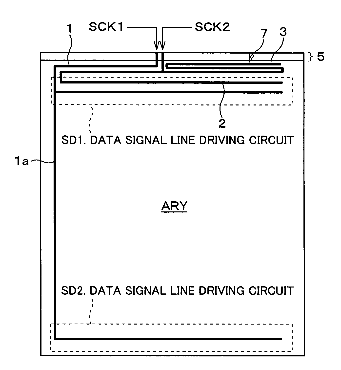
[0051]One embodiment of the present invention will be described below with reference to FIGS. 1 through 9(b).

[0052]Present embodiment uses an active-matrix-type liquid crystal display device as an example of the display device of the present invention.

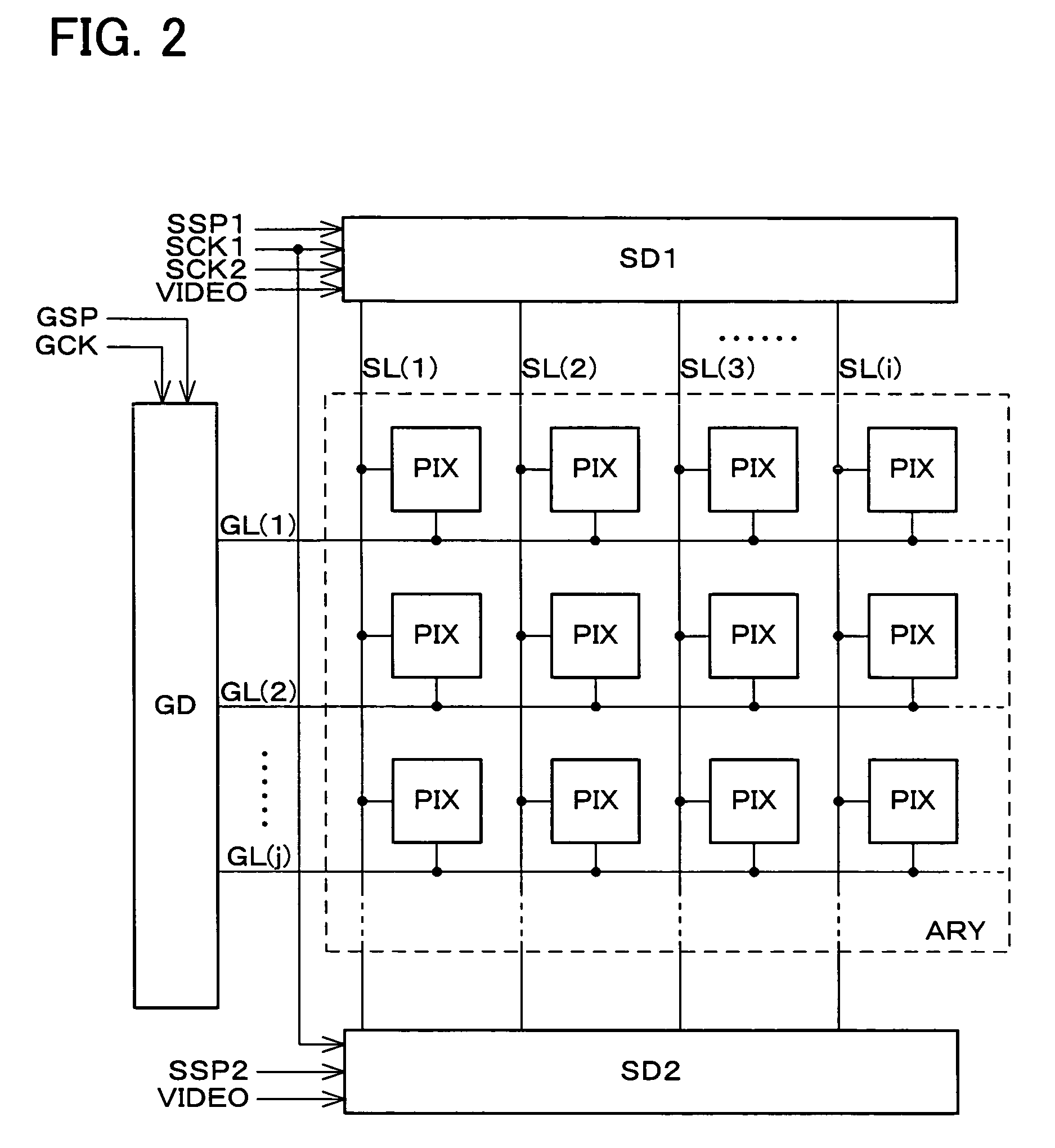
[0053]As shown in FIG. 2, the active-matrix-type liquid crystal display device according to the present invention includes a pixel array ARY, a scanning signal line driving circuit GD1, and two (first and second) data signal line driving circuit SD1 and SD2 which are respectively provided on both sides of the pixel array ARY.

[0054]The pixel array ARY includes a plurality of scanning signal line GL (1) through GL (j) and a plurality of data signal lines SL (1) through SL (i) intersecting with each other, and each square created by two adjacent scanning signal lines GL and two adjacent data signal lines SL is provided with a pixel PIX. Thus, the pixels PIX are aligned in a matrix manner.

[0055]The first and second data signal line driving...


PUM


Abstract

In a structure in which a plurality of signals related to each other are supplied to a driving circuit in such a manner that at least one of the signals is supplied also to the other circuit, the present invention prevents change of phase relation between the plural signals due to difference in wiring load, without directly processing the signals with higher power consumption. The first and second clock signals SCK1 and SCK2 are supplied to the first data signal line driving circuit SD1, while the first clock signal SCK1 is also supplied to the second data signal line driving circuit SD2 in parallel. The wirings 1 and 2 for the respective signals are adjusted to have equal wiring load with a dummy wiring 2 provided in the wiring 2, for solving uneven wiring load caused by difference of leading manner, the dummy wiring 2 constituting an additional capacitor section 7, together with a liquid crystal layer and a counter electrode.

Description

[0001]This Nonprovisional application claims priority under 35 U.S.C. § 119 (a) on Patent Application No. 2002 / 363037 filed in Japan on Dec. 13, 2002, the entire contents of which are hereby incorporated by reference.FIELD OF THE INVENTION[0002]The present invention relates to a display device including a scanning signal line driving circuit for driving a plurality of scanning signal lines and a data signal line driving circuit for driving a plurality of data signal lines intersecting with the scanning signal lines, the display device being suitably used for such as an active-matrix-type liquid crystal display device.BACKGROUND OF THE INVENTION[0003]There has been conventionally known a liquid crystal display device driven by an active matrix manner, as one type of display devices. Note that, the present specification describes a liquid crystal display device as an example of the display device according to the present invention; however, the present invention is not limited to this...

Claims


Application Information

Patent Timeline
IPC IPC(8): G09G3/36G06F3/038G09G5/00G02F1/133G02F1/1345G09G3/20
CPCG09G3/3688G09G3/3607G09G3/3677G09G2330/021G09G2310/0248G09G2320/0223G09G2300/043G09G3/36
Inventor WASHIO, HAJIMEMAEDA, KAZUHIROONDA, MAMORU
Owner SHARP KK
Why Eureka
Try Eureka