Supercharge Your Innovation With Domain-Expert AI Agents!

Connector mounting structure and electronic apparatus having the same

a technology of connecting structure and mounting structure, which is applied in the direction of coupling device details, electrical apparatus casing/cabinet/drawer, coupling device connection, etc., can solve the problems of large terminal displacement, limit the circuit board circuit density, and other components cannot be mounted to the back surface of the board, so as to improve connection reliability and circuit density

Inactive Publication Date: 2008-09-02
DENSO CORP
View PDF9 Cites 26 Cited by
  • Summary
  • Abstract
  • Description
  • Claims
  • Application Information

AI Technical Summary

Benefits of technology

The present invention provides a connector mounting structure that improves connection reliability and circuit density. The structure includes a circuit board, a surface mount connector, and an electronic component. The connector has a base portion and a tube portion with conductive terminals that are connected to the circuit board. The electronic component is mounted on the back surface of the circuit board and partially received in the tube portion. This reduces the risk of displacement of the terminals and improves connection reliability. The space between the circuit board and the first opening portion of the tube portion increases circuit density, allowing for a smaller circuit board size. The invention also provides an electronic apparatus with this connector mounting structure.

Problems solved by technology

Since the terminal of the connector is exposed to a back surface of the board, other components cannot be mounted to the back surface of the board, directly beneath the through hole.
Therefore, the through-hole mounting structure limits circuit density of the circuit board.
Therefore, displacement of the terminal relative to the connector body causes large displacement of the terminal relative to the land formed on the circuit board.
It is difficult to ensure the connection reliability between the connector and the circuit board.

Method used


Image

  • Connector mounting structure and electronic apparatus having the same
  • Connector mounting structure and electronic apparatus having the same
  • Connector mounting structure and electronic apparatus having the same

Examples


first embodiment

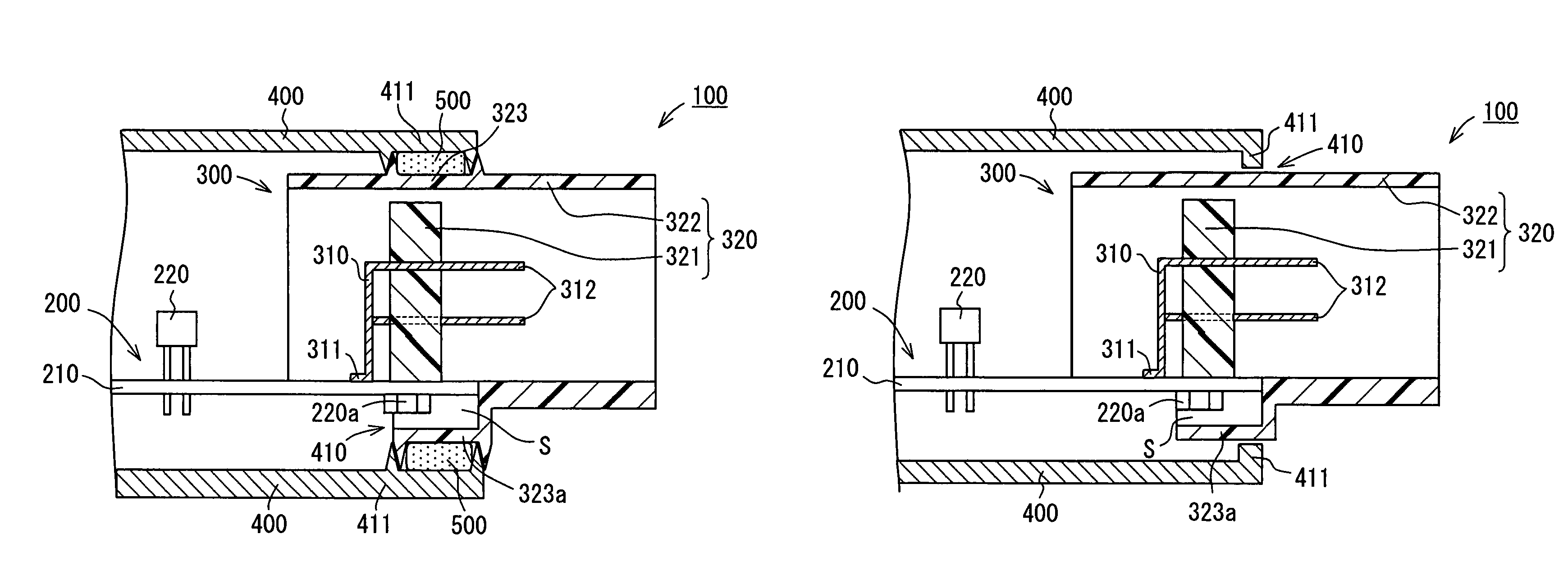
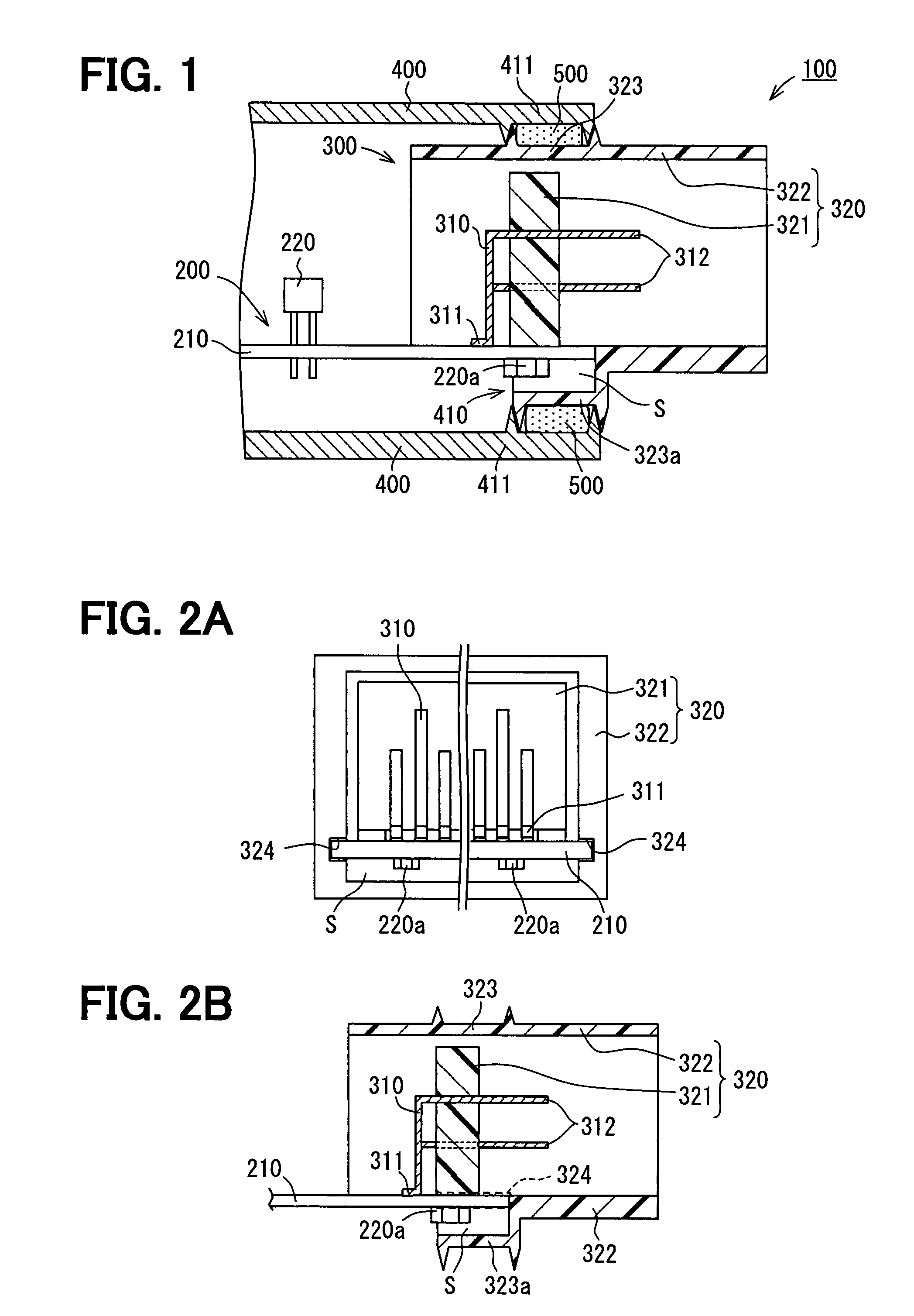
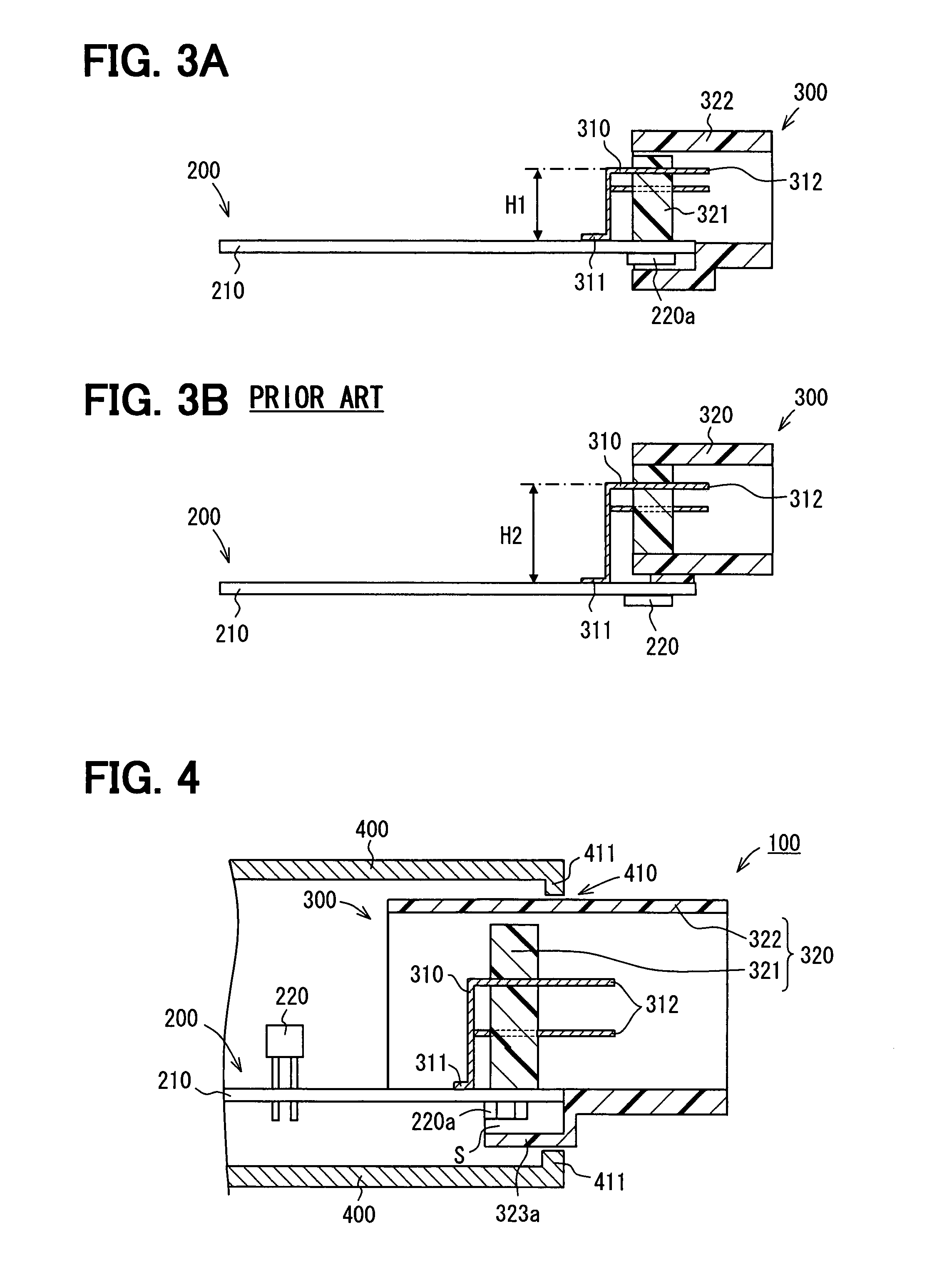
[0022]As shown in FIG. 1, an electronic apparatus 100 includes a circuit board 200, a surface mount connector 300 mounted to the circuit board 200, and a housing 400 for holding the circuit board 200 therein. The housing 400 is sealed by a sealant 500 so that the circuit board 200 held in the housing 400 is protected from water. Thus, the electronic apparatus 100 is waterproof and is suitable for use in an electronic control unit (ECU) installed in an engine room of a vehicle, for example.

[0023]The circuit board 200 includes a printed board 210 and an electronic element 220 mounted to the printed board 210. The printed board 210 has wiring patterns and via holes connecting the wiring patterns. The printed board 210 may be, for example, made of thermoplastic resin, thermoset resin, ceramic, glass-resin composite (e.g., glass cloth), or the like. In the first embodiment, the printed board 210 is a multilayer board including multiple inner layers, each of which includes a wiring patter...

second embodiment

[0047]The second embodiment of the present invention is shown in FIG. 8 and FIG. 9A, 9B. In the first embodiment described previously, as shown in FIG. 1, the electronic component 220a is mounted to the back surface of the printed board 210, approximately beneath the base portion 321. In contrast, in the second embodiment, as shown in FIG. 8, the electronic component 220a is mounted to a back surface 212 of the printed board 210, approximately beneath a conductive land 213 to which the terminal 310 is soldered. The terminal 310 and the electronic component 220a are connected to each other by a via hole 214 and a wiring member 215. Since the electronic component 220a is mounted approximately beneath the land 213, the length of the wiring member 215 can be greatly reduced so that the wiring impedance can be greatly reduced.

[0048]Further, as shown in FIGS. 9A and 9B, a power terminal 310a and a ground terminal 310b of the terminals 310 are arranged adjacent to each other in a direction...

third embodiment

[0050]The third embodiment of the present invention is shown in FIG. 10. The tube portion 322 has an extension portion 326 extending from the inner surface of the tube portion 322 toward the back surface of the circuit board 200. Thus, the space S is divided into spaces S1, S2 by the extension portion 326. At least one electronic component 220a is arranged in each of the spaces S1, S2. The extension portion 326 supports the circuit board 200 to increase stiffness of the connector 300. Alternatively, the tube portion 322 has three extension portions 326 extending from the inner surface of the tube portion 322 toward the back surface of the circuit board 200. Thus, the space S is divided into spaces S1, S2, S3, S4 by the extension portions 326. At least one electronic component 220a is arranged in each of the spaces S1, S2, S3, S4. In such an approach, the stiffness of the connector 300 can be more increased. As the size of each space is small, the stiffness of the connector 300 is in...


PUM


Abstract

A connector mounting structure includes a circuit board, a surface mount connector mounted to the circuit board, and an electronic component. The connector includes a connector body and a plurality of conductive terminals. The connector body has a base portion placed on a front surface of the circuit board and a tube portion. The terminals are disposed in the base portion of the connector body. The tube portion has a first opening portion for partially receiving the circuit board and a second opening portion for communicating with an external device. The electronic component is mounted to a back surface of the circuit board. A space for the electronic component is provided approximately beneath the base portion, between the back surface of the circuit board and the first opening portion of the tube portion.

Description

CROSS REFERENCE TO RELATED APPLICATION[0001]This application is based on and incorporates herein by reference Japanese Patent Application No. 2006-55383 filed on Mar. 1, 2006.FIELD OF THE INVENTION[0002]The present invention relates to a connector mounting structure and an electronic apparatus having the mounting structure.BACKGROUND OF THE INVENTION[0003]In a conventional through-hole mounting structure disclosed in, for example, U.S. Pat. No. 6,707,678 corresponding to JP-3669224, each terminal of a connector is inserted into a through hole formed in a circuit board. A conductive land is formed on an inner wall of the hole and formed on a front surface of the board around an opening of the hole. The terminal of the connector is soldered to the land in a reflow process so that the connector is electrically and mechanically connected to the circuit board. Thus, the connector is mounted to the front surface of the board. Since the terminal of the connector is exposed to a back surfac...

Claims


Application Information

Patent Timeline
Patent Type & Authority Patents(United States)
IPC IPC(8): H01R12/00
CPCH01R12/724H01R23/70H01R13/6616H01R13/6625H01R12/707H05K5/0069H01R12/00
Inventor ITOU, DAIMIKURA, HIDEHIROITO, ATSUSHIHONDA, TAKAYOSHITSURUZAWA, TADASHI
Owner DENSO CORP
Features
  • R&D
  • Intellectual Property
  • Life Sciences
  • Materials
  • Tech Scout
  • Unparalleled Data Quality
  • Higher Quality Content
  • 60% Fewer Hallucinations
Learn More