Unlock instant, AI-driven research and patent intelligence for your innovation.

Non-volatile semiconductor memory device

a non-volatile, semiconductor technology, applied in static storage, digital storage, instruments, etc., can solve the problems of small power consumption, remained a danger of write disturbance (erroneous write) in non-selected cells, and erroneous wri

Inactive Publication Date: 2008-09-02
KK TOSHIBA
View PDF10 Cites 9 Cited by
  • Summary
  • Abstract
  • Description
  • Claims
  • Application Information

AI Technical Summary

Benefits of technology

The present invention provides a non-volatile semiconductor memory device with a NAND cell unit that includes multiple electrically rewritable and non-volatile memory cells connected in series. The device includes a source line and a bit line, and the NAND cell unit is biased in a data write mode by applying a write voltage to the control gate of a selected memory cell, a channel-isolating voltage to control gates of non-selected memory cells on the source line side of the selected memory cell, and a write medium voltage to control gates of non-selected memory cells at intervals of a certain number of memory cells. The method of writing the device involves controlling the channel potential of a selected memory cell and applying a write voltage and a write medium voltage to the control gate of the selected memory cell and control gates of non-selected memory cells, respectively. The technical effects of the invention include improved data write efficiency and reliability.

Problems solved by technology

Further, since data write is performed with F-N tunneling current, the power consumption is small.
However, in case the non-selected cell is set at 0[volts], which is disposed just adjacent to the selected cell with the write voltage Vpgm applied, a leakage current is generated due to band-to-band tunneling at the drain edge of the non-selected cell with the channel separating or isolating voltage, 0V, applied, and it is possible to cause erroneous write.
However, in the self boost scheme provided in the prior art, there is remained a danger of write disturbance (erroneous write) in the non-selected cells.

Method used


Image

  • Non-volatile semiconductor memory device
  • Non-volatile semiconductor memory device
  • Non-volatile semiconductor memory device

Examples


embodiment 1

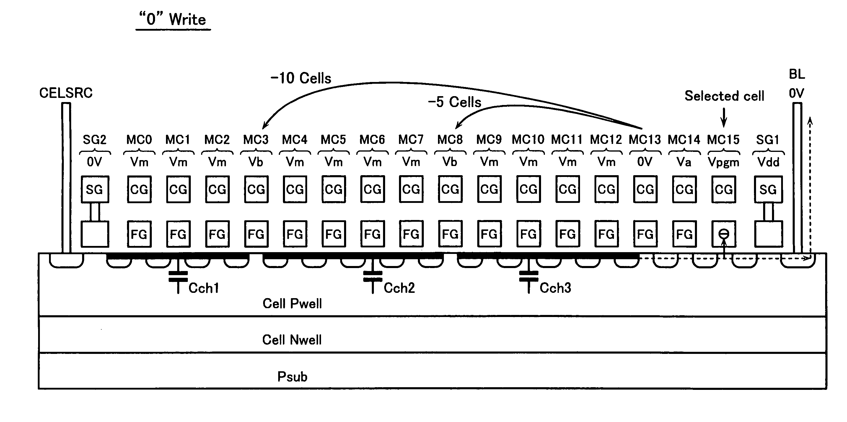
[0062]FIG. 4 shows the entire and schematic composition of the NAND-type flash memory in accordance with this embodiment. NAND cell unit (i.e., NAND string) 100, which is a basic unit of the NAND-type flash memory, has a plurality of electrically rewritable and non-volatile memory cells MC0-MC31 connected in series, and two select gate transistors SG1 and SG2 disposed at both end thereof. One end of the NAND cell unit 100 is coupled to bit line BL via the select gate transistor SG1; and the other end to source line CELSRC via the select gate transistor SG2.

[0063]One memory cell has, as well known, N-type source / drain diffusion areas formed on the P-type well of a silicon substrate, and a stacked gate structure with a floating gate serving as a charge storing layer and a control gate. Changing the quantity of charge in the floating gate based on write / erase operations and changing the threshold voltage of the memory cell, the memory cell stores data of one bit or multiple bits.

[0064]...

embodiment 2

[0118]In the above-described Embodiment 1, the positions of cells, to which the channel-isolating voltage Vb is applied, are relatively determined on the basis of the cell with the channel isolating-voltage Vc(=0[volts] applied. By contrast, in the Embodiment 2 shown in FIGS. 12 and 13, the NAND cell unit is classified into some groups with the same cell numbers, and the channel-isolating voltage Vb is applied to at least one lo memory cell (i.e., word line) in each group, the position of which is fixed in the group.

[0119]However, with respect to a group neighboring on the cell source line side of that including the selected cell, the voltage Vb is not applied because there is a cell with the channel-isolating voltage Vc=0[volts] applied within or at least near the group in accordance with the selected cell position.

[0120]In the example shown in FIGS. 12 and 13, the number of cells in the NAND cell unit is sixteen, and the cells are divided into four groups, Group1-4. FIGS. 12 and 1...

embodiment 3

[0122]As an embodiment, an electric card using the non-volatile semiconductor memory devices according to the above-described embodiments of the present invention and an electric device using the card will be described bellow.

[0123]FIG. 14 shows an electric card according to this embodiment and an arrangement of an electric device using this card. This electric device is a digital still camera 101 as an example of portable electric devices. The electric card is a memory card 61 used as a recording medium of the digital still camera 101. The memory card 61 incorporates an IC package PK1 in which the non-volatile semiconductor memory device or the memory system according to the above-described embodiments is integrated or encapsulated.

[0124]The case of the digital still camera 101 accommodates a card slot 102 and a circuit board (not shown) connected to this card slot 102. The memory card 61 is detachably inserted in the card slot 102 of the digital still camera 101. When inserted in ...


PUM


Abstract

A non-volatile semiconductor memory device including a NAND cell unit with a plurality of electrically rewritable and non-volatile memory cells connected in series, a source line coupled to one end of the NAND cell unit, and a bit line coupled to the other end of the NAND cell unit, wherein the NAND cell unit is biased in a data write mode as follows: a write voltage Vpgm is applied to a control gate of a selected memory cell in the NAND cell unit; a channel-isolating voltage is applied to control gates of non-selected memory cells disposed on the source line side of the selected memory cell at intervals of a certain number of memory cells; and a write medium voltage Vm lower than Vpgm is applied to control gates of the remaining non-selected memory cells.

Description

CROSS-REFERENCE TO RELATED APPLICATION[0001]This application is based on and claims the benefit of priority from the prior Japanese Patent Application No. 2005-251988, filed on Aug. 31, 2005, the entire contents of which are incorporated herein by reference.BACKGROUND OF THE INVENTION[0002]1. Field of the Invention[0003]This invention relates to an electrically rewritable and non-volatile semiconductor memory device (EEPROM), especially relates to a NAND-type flash memory.[0004]2. Description of the Related Art[0005]A NAND-type flash memory is known as one of EEPROMs. In the NAND-type flash memory, multiple memory cells are connected in series in such a way that adjacent two memory cells share a source / drain diffusion area, thereby constituting a NAND cell unit. Therefore, the unit cell area is made smaller than that of a NOR-type flash memory, and it is easy to achieve a large capacity. Further, since data write is performed with F-N tunneling current, the power consumption is smal...

Claims


Application Information

Patent Timeline
Patent Type & Authority Patents(United States)
IPC IPC(8): G11C16/04
CPCG11C11/5628G11C16/0483G11C16/32G11C16/12G11C2211/565G11C16/02G11C16/30
Inventor HOSONO, KOJI
Owner KK TOSHIBA