Copper adhesion improvement device and method

a technology of adhesion improvement and copper wire, which is applied in the direction of semiconductor devices, semiconductor/solid-state device details, electrical devices, etc., can solve the problems of high difficulty in manufacturing methods, resistance of copper wiring rises, and problems that cannot be solved, so as to improve the em tolerance of wiring structure and improve the adhesion

Active Publication Date: 2008-09-09
KIOXIA CORP
View PDF13 Cites 2 Cited by
  • Summary
  • Abstract
  • Description
  • Claims
  • Application Information

AI Technical Summary

Benefits of technology

[0015]An aspect of the present invention is provided to make a proposal of a semiconductor device which can improve the adhesion between a copper wiring and a stopper and the adhesion between a copper wiring and a barrier metal without bringing about a new problem such as a problem on process, a problem of wiring resistance, or the like, and is to make an attempt to improve an EM tolerance of the wiring structuring an LSI.

Problems solved by technology

However, in this technique, a metal 4 must be selectively formed on the copper wiring 1 by using, for example, a CVD method, an electrolytic plating method, or the like, and the problem that technical difficulty with respect to the manufacturing method is made high arises.
However, the problems cannot be solved without any problem of process.
However, a new problem that, if the additive is uniformly included in the entire copper wiring, the resistance of the copper wiring rises occurs.
Namely, the reliability of the wiring (the improvement in the EM tolerance) and a signal delay (a deterioration in wiring resistance) establish the relationship of trade-off, and as a result, a high performance and high reliability multi-level interconnection structure cannot be provided.

Method used


Image

  • Copper adhesion improvement device and method
  • Copper adhesion improvement device and method
  • Copper adhesion improvement device and method

Examples


first embodiment

(1) First Embodiment

[0052]FIGS. 6 to 11 show a manufacturing method for a semiconductor device according to a first embodiment of the present invention.

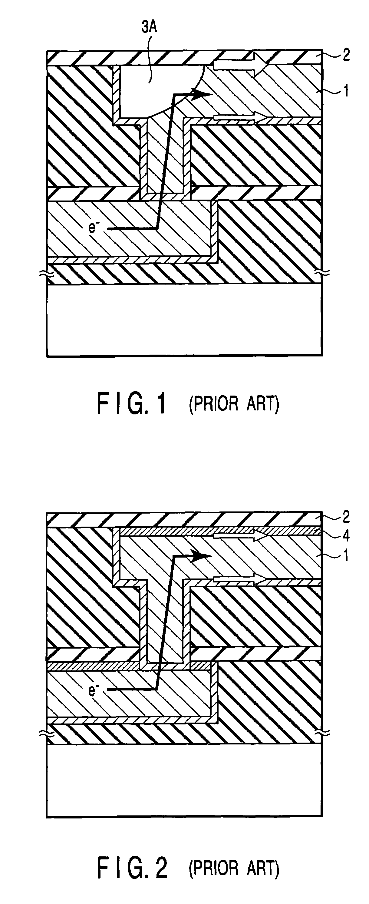
[0053]First, as shown in FIG. 6, a wiring slot is formed on an insulating layer (for example, silicon oxide) 12 on a silicon substrate 11 by using a method such as, for example, PEP (Photo Engraving Process), or RIE (Reactive Ion Etching).

[0054]A barrier metal 13 for covering the bottom surfaces and the side surfaces of the wiring slot is formed on the insulating layer 12 by using a method such as a CVD method or a PVD method. Next, a seed copper (seed-Cu) 14′ serving as a seed layer which will be undercoating at the time of copper plating is formed on the barrier metal 13 by, for example, a sputtering method. Thereafter, a copper plate layer 14 having a sufficient thickness for filling up the wiring slot is formed on the seed copper 14′ by using, for example, an electrolytic plating method.

[0055]Note that, after the process of coppe...

second embodiment

(2) Second Embodiment

[0067]FIGS. 14 to 17 show a manufacturing method for a semiconductor device according to a second embodiment of the present invention.

[0068]First, as shown in FIG. 14, a wiring slot is formed on the insulating layer (for example, silicon oxide) 12 on the silicon substrate 11 by using a method such as, for example, PEP or RIE.

[0069]The barrier metal 13 for covering the bottom surfaces and the side surfaces of the wiring slot is formed on the insulating layer 12 by using a method such as a CVD method or a PVD method.

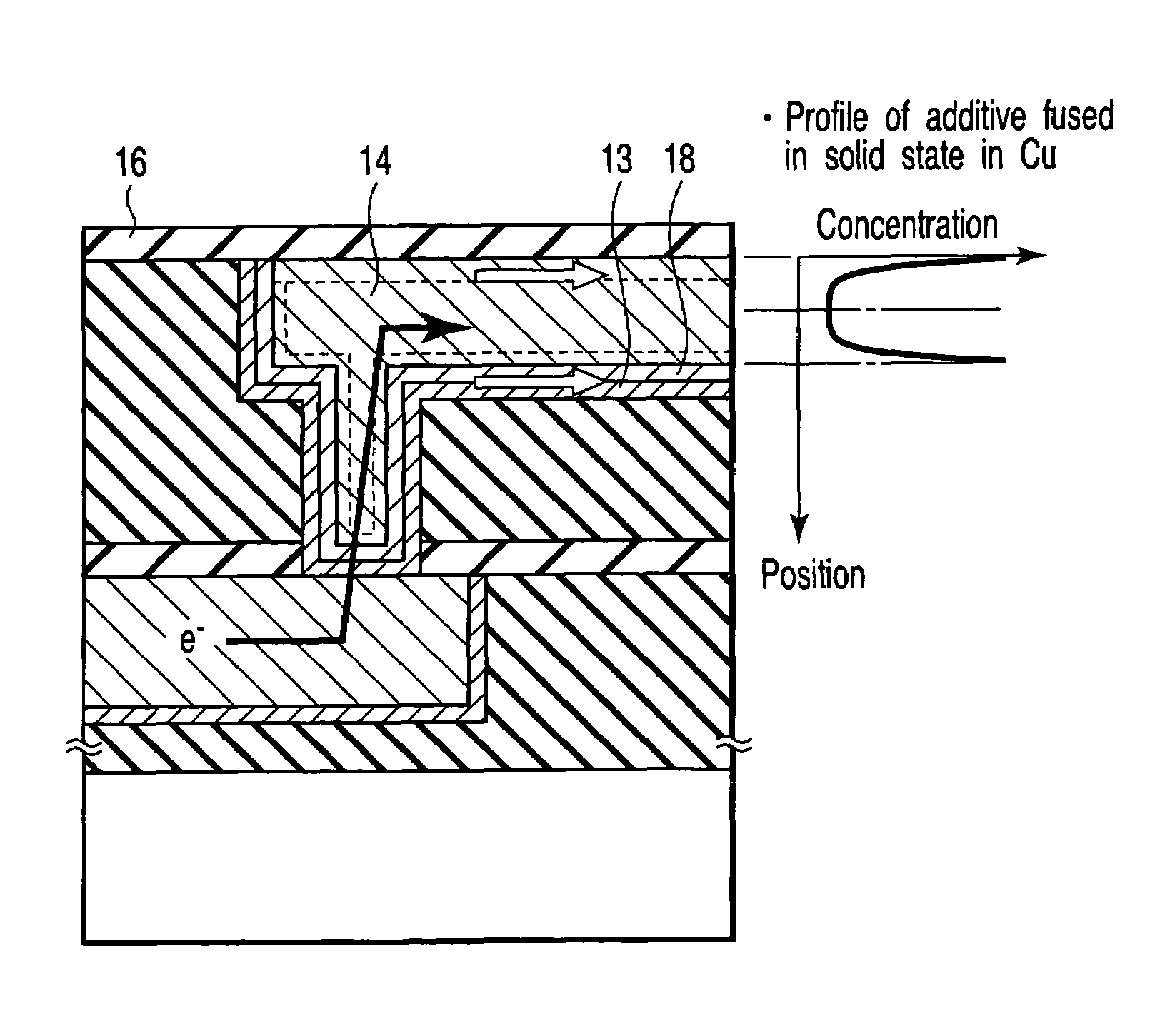
[0070]Thereafter, a layer 18 of a material solid-soluble in copper made of an additive which is fused in a solid state in copper, and by which the adhesion with the barrier metal 13 and a stopper (an insulating layer of SiN, SiCN, SiCO, SiC or the like) which will be described later can be improved, for example, Ti, Al, Si, Co, B or P, or the layer 18 of a material solid-soluble in copper including one of those additives is formed on the barrier metal ...


PUM


Abstract

A semiconductor device, in which a semiconductor integrated circuit having a multi-level interconnection structure is formed, according to an embodiment of the present invention, comprises a copper wiring and an insulating layer formed on a top surface of the copper wiring, wherein the copper wiring includes an additive for improving adhesion between the copper wiring and the insulating layer, and a profile of the additive has a gradient in which a concentration is gradually reduced as it goes from the top surface of the copper wiring toward the inside thereof, and has the highest concentration on the top surface of the copper wiring.

Description

CROSS-REFERENCE TO RELATED APPLICATIONS[0001]This application is based upon and claims the benefit of priority from prior Japanese Patent Application No. 2004-351680, filed Dec. 3, 2004, the entire contents of which are incorporated herein by reference.BACKGROUND OF THE INVENTION[0002]1. Field of the Invention[0003]The present invention relates to a semiconductor device such as a memory LSI of which a logic LSI (Logical Large Scale Integrated Circuit), a DRAM (Dynamic Random Access Memory), and an SRAM (Static Random Access Memory) are typical, an LSI configured by a bipolar transistor, or the like.[0004]2. Description of the Related Art[0005]In recent years, as a wiring structure of an LSI, a multi-level interconnection structure using a copper (Cu) damascene wiring (a copper wiring formed by a damascene process) has joined the mainstream due to the demands for making an LSI minute and low-resistant, and the like. Copper wiring generally has higher electro-migration (EM) tolerance ...

Claims


Application Information

Patent Timeline
Patent Type & Authority Patents(United States)
IPC IPC(8): H01L21/4763
CPCH01L21/76834H01L21/76843H01L21/76867H01L21/76849H01L21/76864H01L21/76846Y10S438/927
Inventor HIGASHI, KAZUYUKIYAMADA, MASAKIMATSUNAGA, NORIAKI
Owner KIOXIA CORP
Why Eureka
Try Eureka