Semiconductor substrates including vias of nonuniform cross section, methods of forming and associated structures

a technology of semiconductors and substrates, applied in the direction of semiconductor devices, semiconductor/solid-state device details, electrical apparatus, etc., can solve the problems of compromising the reliability of the system they inhabit, requiring an additional processing step and additional equipment, and allowing the expansion of the solvent outsid

Active Publication Date: 2008-09-16
MICRON TECH INC
View PDF13 Cites 19 Cited by
  • Summary
  • Abstract
  • Description
  • Claims
  • Application Information

AI Technical Summary

Problems solved by technology

Such pockets may cause the solder to expand outside the via.
If large enough, these voids can compromise reliability in the systems they inhabit by impairing an electrical connection or providing a connection which may fail later during use.
A hole may be laser-drilled to the bottom of a blind via to provide a vent for the flux gases; however, this requires an additional processing step and additional equipment.
The contact between the conductive material of a via and a solder ball may create a brittle solder joint line susceptible to failure.

Method used


Image

  • Semiconductor substrates including vias of nonuniform cross section, methods of forming and associated structures
  • Semiconductor substrates including vias of nonuniform cross section, methods of forming and associated structures
  • Semiconductor substrates including vias of nonuniform cross section, methods of forming and associated structures

Examples


Embodiment Construction

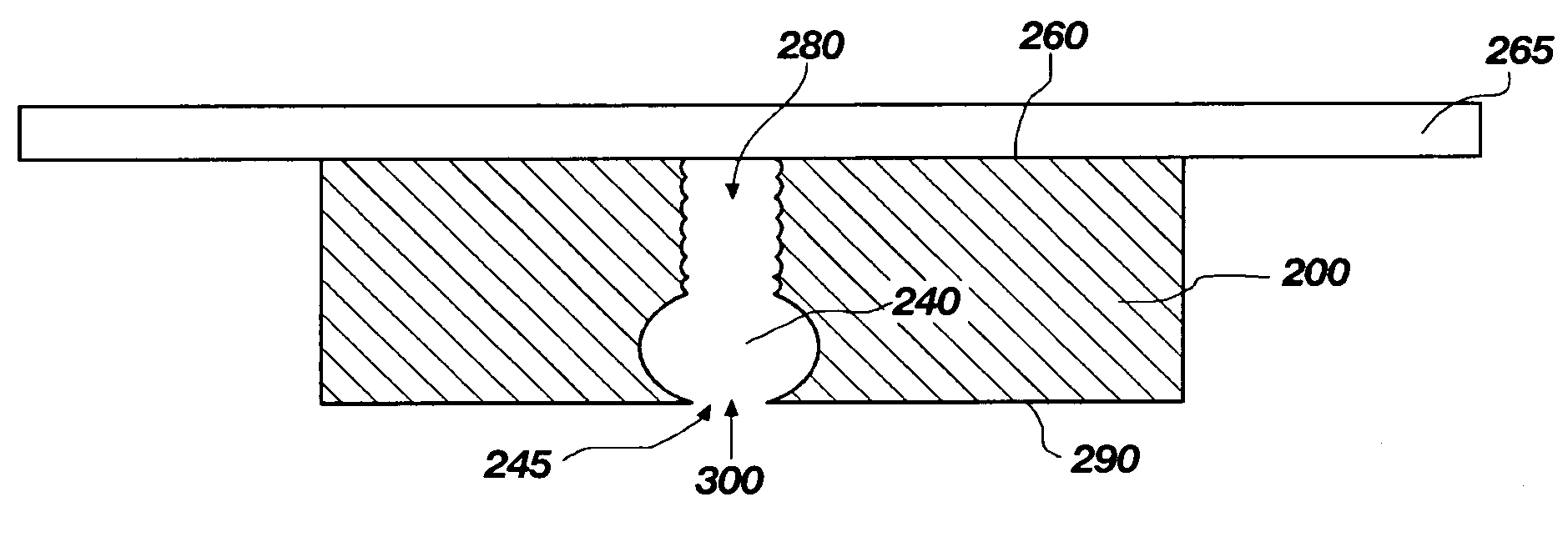
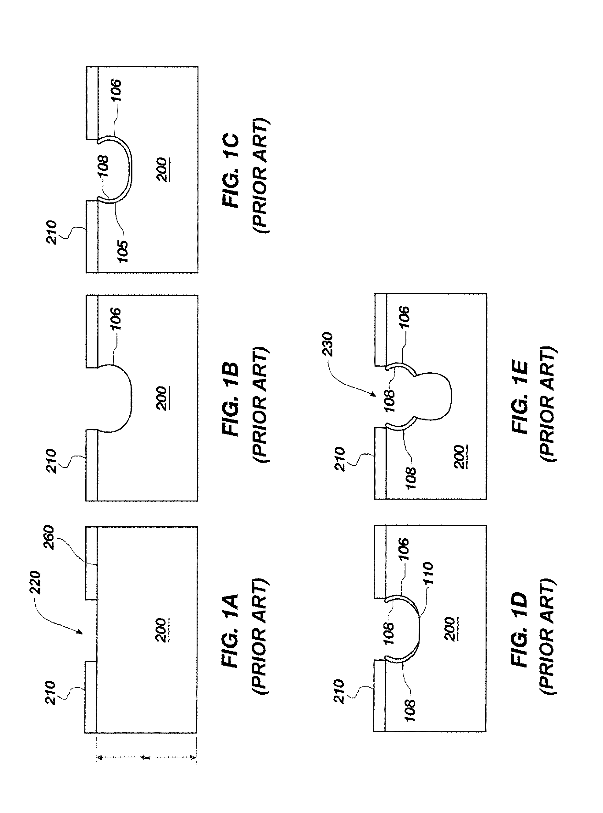
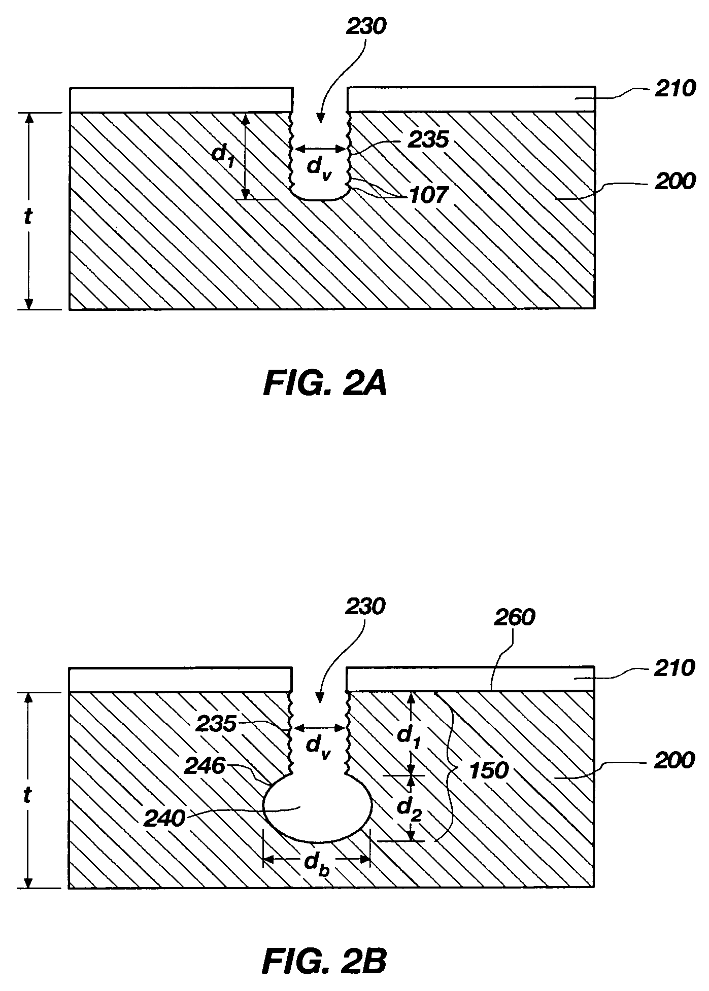
[0020]Referring in general to the accompanying drawings, various aspects of the present invention are illustrated to show exemplary wafers including through-hole vias, vias with conductive material disposed therein and conductive elements positioned thereon, as well as methods of forming vias. Common elements of the illustrated embodiments are designated with like reference numerals for clarity. It should be understood that the figures presented are not meant to be illustrative of actual views of any particular portion of a particular wafer, but are merely idealized schematic representations which are employed to more clearly and fully depict the invention. It will be apparent by those of ordinary skill in the art that while the methods and structures disclosed herein describe methods for fabricating vias, the acts and structures described herein comprise a portion of an entire fabrication process of a semiconductor device or other substrate and may be used in combination with other...


PUM


Abstract

Methods for forming a via and a conductive path are disclosed. The methods include forming a via within a wafer with cyclic etch / polymer phases, followed by an augmented etch phase. The resulting via may include a first portion having a substantially uniform cross section and a second portion in the form of a hollow ball, extending laterally further within the wafer than the first portion. Back-grinding the wafer to the second portion of the via may create a vent. A conductive path may be formed by filling the via with a conductive material, such as solder. Flux gases may escape through the vent. The wafer surrounding the second portion of the via may be removed, exposing a conductive element in the shape of a ball, the shape of the second portion of the via. Semiconductor devices including the conductive paths of the present invention are also disclosed.

Description

BACKGROUND OF THE INVENTION[0001]1. Field of the Invention[0002]The present invention relates generally to the field of semiconductor device fabrication and, more particularly, to wafers having vias formed therein. Methods of forming vias, including vented vias and vias filled with conductive material and having conductive elements thereon are also included.[0003]2. Background of Related Art[0004]Semiconductor chips may be produced with integrated circuits on one or (less commonly) both sides of the chip and may be designed to connect to or interact with other electronic components or other semiconductor chips. Interposers may be utilized for interfacing two electrical components, such as a semiconductor device and a printed circuit board, and contactor boards may be used to interface a semiconductor wafer and a probe card for testing the dice on the semiconductor wafer. Semiconductor chips may be formed of semiconductor wafer or other bulk semiconductor substrate material, while in...

Claims


Application Information

Patent Timeline
Patent Type & Authority Patents(United States)
IPC IPC(8): H01L21/311
CPCH01L21/30655H01L21/76898H01L23/481H01L21/312H01L2924/09701H01L2224/16227H01L2224/11H01L2224/13H01L2224/13009H01L2224/16146H01L2224/16225H01L2224/05573H01L2224/13025H01L2924/00014H01L2224/0554H01L21/02282H01L21/0214H01L21/02118H01L21/0217H01L21/02164H01L2224/05599H01L2224/0555H01L2224/0556
Inventor LAKE, RICKIE C.
Owner MICRON TECH INC
Why Eureka
Try Eureka