Multiple level minimum logic network

a logic network and multi-level technology, applied in data switching networks, instruments, architectures with multiple processing units, etc., can solve the problems of computational units idle, ring and mesh networks are plagued by lengthy delay in message communication, and the latency of accessing another computational unit is increased, so as to minimize processing and storage overhead at each node, the effect of high bandwidth and low latency

Inactive Publication Date: 2008-09-16
INTERACTIC HLDG LLC
View PDF4 Cites 9 Cited by
  • Summary
  • Abstract
  • Description
  • Claims
  • Application Information

AI Technical Summary

Benefits of technology

[0008]In accordance with the present invention, a multiple level minimum logic network interconnect structure has a very high bandwidth and low latency. Control of interconnect structure switching is distributed throughout multiple nodes in the structure so that a supervisory controller providing a global control function is not necessary. A global control function is eliminated and complex logic structures are avoided by a novel data flow technique that is based on timing and positioning of messages communicating through the interconnect structure. Furthermore, the interconnect structure implements a “deflection” or “hot potato” design in which processing and storage overhead at each node is minimized by routing a message packet through an additional output port rather than holding the packet until a desired output port is available. Accordingly, the usage of buffers at the nodes is eliminated. Elimination of a global controller and buffering at the nodes greatly reduces the amount of control and logic structures in the interconnect structure, simplifying overall control components and network interconnect components, improving speed performance of message communication and potentially reducing interconnection costs substantially. Implementation of the interconnect structure is highly flexible so that fully electronic, fully optical and mixed electronic-optical embodiments are achieved. An implementation using all optical switches is facilitated by nodes exploiting uniquely simple logic and elimination of buffering at the nodes.
[0035]The disclosed multiple level interconnect structure has many advantages. One advantage is that the structure is simple, highly ordered and achieves fast and efficient communication for systems having a wide range of sizes, from small systems to enormous systems.
[0036]In addition, the interconnect structure is highly advantageous for many reasons. The interconnect structure resolves contention among messages directed toward the same node and ensures that a message that is blocked makes a complete tour of the nodes on a level before the blocking message is in position to block again. In this manner, a message inherently moves to cover all possible paths to the next level. A blocking message typically proceeds to subsequent levels so that overlying messages are not blocked for long.

Problems solved by technology

One disadvantage of a network connection is an increase in the latency of access to another computational unit since transmission of a message traverses several stages of a network.
Unfortunately, the ring and mesh networks typically are plagued by lengthy delays in message communication since the number of nodes traversed in sending a message from one node to another may be quite large.
These lengthy delays commonly cause a computational unit to remain idle awaiting a message in transit to the unit.
Circuit switching disadvantageously requires a lengthy setup time.
Such delays are intolerable during the short and quick exchanges that take place between different computational units.
Furthermore, a dedicated pathway is very wasteful of system bandwidth.
Because no transmission capacity is specifically reserved for an individual computational unit, time gaps between packets are filled with packets from other users.

Method used


Image

  • Multiple level minimum logic network
  • Multiple level minimum logic network
  • Multiple level minimum logic network

Examples


Embodiment Construction

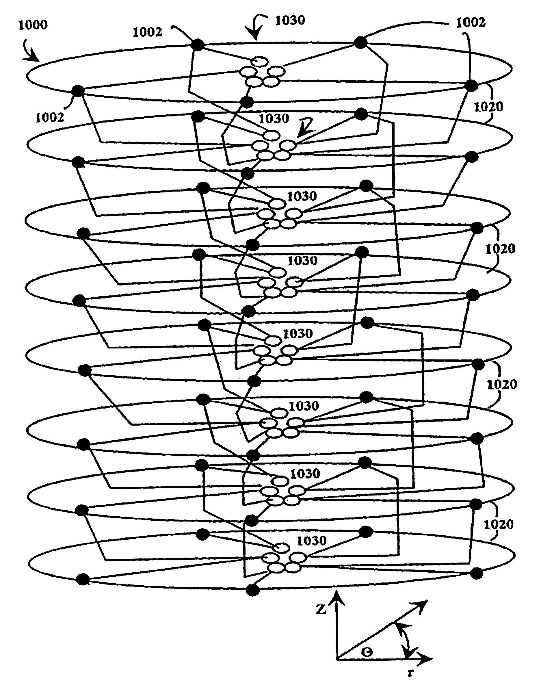
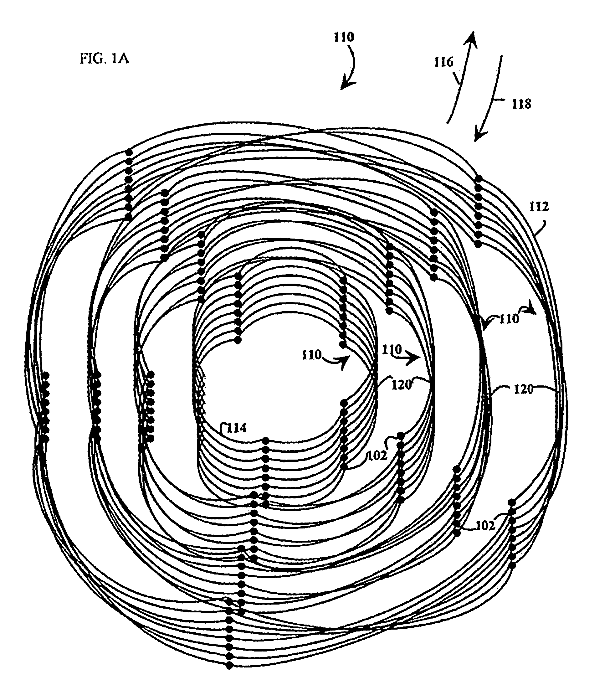
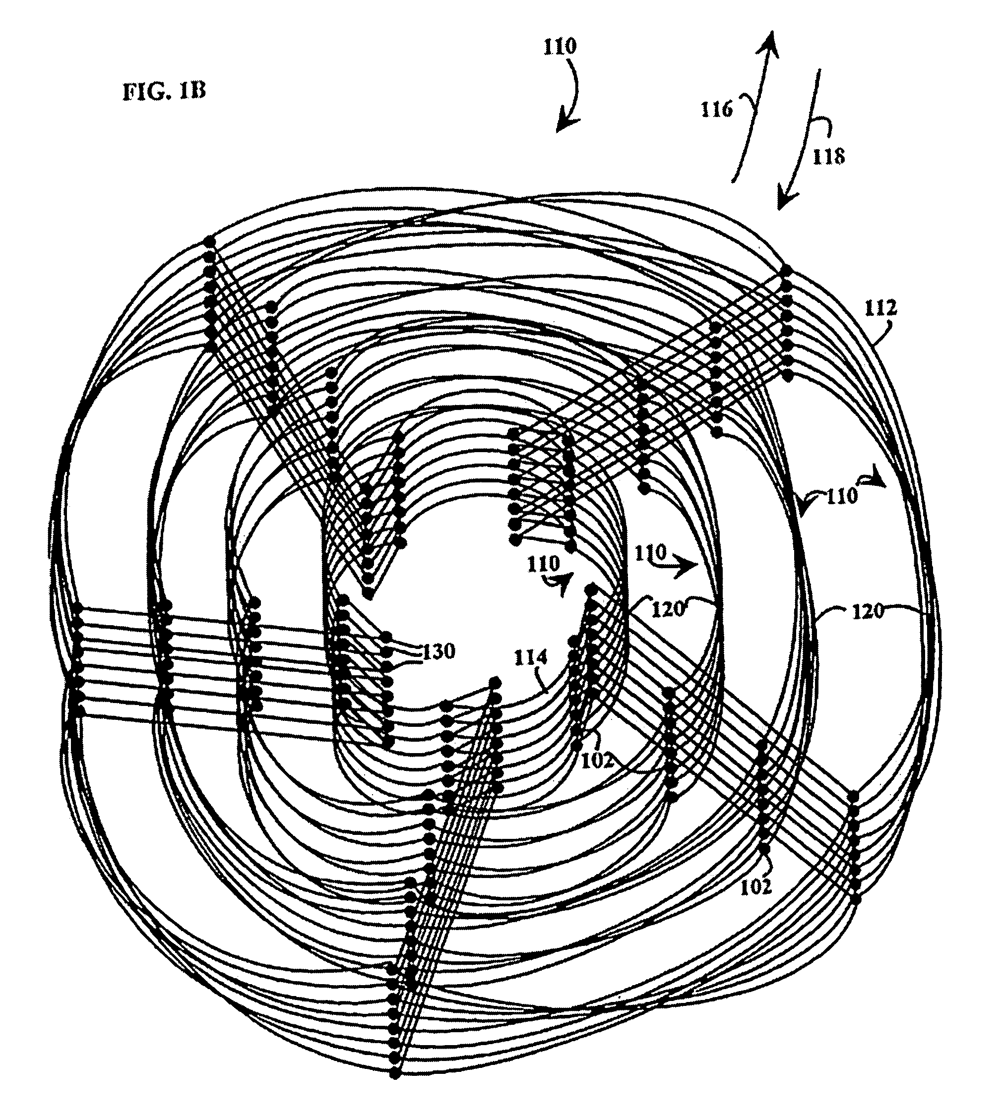
[0063]Referring to FIGS. 1A, 1B, 1C and 1D, an embodiment of a multiple level minimum logic interconnect apparatus 100 includes multiple nodes 102 which are connected in a multiple level interconnect structure by interconnect lines. The multiple level interconnect structure is shown illustratively as a three−dimensional structure to facilitate understanding.

[0064]The nodes 102 in the multiple level interconnect structure are arranged to include multiple levels 110, each level 110 having a hierarchical significance so that, after a message is initiated in the structure, the messages generally move from an initial level 112 to a final level 114 in the direction of levels of a previous hierarchical significance 116 to levels of a subsequent hierarchical significance 118. Illustratively, each level 110 includes multiple structures which are called rings 120. Each ring 120 includes multiple nodes 102. The term “rings” is used merely to facilitate understanding of the structure of a netwo...


PUM


Abstract

A network or interconnect structure 100 utilizes a data flow technique that is based on timing and positioning of messages communicating through the interconnect structure. Switching control is distributed throughout multiple nodes 102 in the structure so that a supervisory controller providing a global control function and complex logic structures are avoided. The interconnect structure operates as a “deflection” or “hot potato” system in which processing and storage overhead at each node is minimized. Elimination of a global controller and buffering at the nodes greatly reduces the amount of control and logic structures in the interconnect structure, simplifying overall control components and network interconnect components 104 and improving speed performance of message communication.

Description

RELATED APPLICATIONS[0001]This application is a continuation of Ser. No. 09 / 852009 filed May 7, 2001 U.S. Pat. No. 7,068,671, a division of U.S. patent application Ser. No. 09 / 850,953, filed May 7, 2001 now abandoned, and a division of Ser. No. 09 / 397333, filed Sep. 14, 1999 U.S. Pat No. 6,272,141 and Ser. No. 08 / 505513 filed Jul. 21, 1995 U.S. Pat. No. 5,996,020, all entitled “Minimum Level Minimum Logic Network”, invented by Coke S. Reed, claiming an earliest effective filing date of Jul. 21, 1995.FIELD OF INVENTION[0002]The present invention relates to interconnection structures for computing and communication systems. More specifically, the present invention relates to multiple level interconnection structures in which control and logic circuits are minimized.BACKGROUND OF THE INVENTION[0003]Many advanced computing systems, including supercomputers for example, utilize multiple computational units to improve performance in what is called a parallel system. The system of intercon...

Claims


Application Information

Patent Timeline
Patent Type & Authority Patents(United States)
IPC IPC(8): H04L12/28H04L12/56G06F15/173G06F15/80H04L12/58
CPCG06F15/17375G06F15/17393H04L45/06H04L12/42G06F15/803G06F15/16
Inventor REED, COKE S.
Owner INTERACTIC HLDG LLC
Why Eureka
Try Eureka