Buffer circuit with enhanced overvoltage protection

a buffer circuit and protection technology, applied in the field of electronic circuits, can solve the problems of consuming significant direct current (dc) power, slowing down the buffer speed, and limiting the minimum vdd range under which the buffer circuit will function properly to less than about two volts, so as to reduce the speed and/or input, and reduce the dc power consumption

Active Publication Date: 2008-09-30
AVAGO TECH INT SALES PTE LTD
View PDF7 Cites 13 Cited by
  • Summary
  • Abstract
  • Description
  • Claims
  • Application Information

AI Technical Summary

Benefits of technology

[0005]The present invention meets the above-noted need by providing, in an illustrative embodiment, an improved buffer circuit having overvoltage protection without significantly reducing a speed and / or input voltage swing of the buffer circuit. Additionally, the improved buffer circuit is configured to have reduced DC power consumption during an overvoltage condition of the buffer circuit.

Problems solved by technology

The inclusion of the NMOS device, however, significantly restricts an input voltage swing of the buffer circuit, which slows down the buffer speed, particularly at lower supply voltages (e.g., about 2.0V).
Additionally, the NMOS device limits the minimum VDD range under which the buffer circuit will properly function to less than about two volts.
Adding a series NMOS protection device between the input pad 102 and the remainder of the buffer circuitry can also cause the buffer circuit to consume significant direct current (DC) power, for example when an input signal applied to the buffer circuit is a logic high level.
Moreover, if the first stage of the buffer circuit, including NMOS device M2 and PMOS device M1, incorporates a low pass filter therein, as is often required in certain applications, a delay through the filter would vary as a function of the incoming bit patterns applied to the buffer circuit, which is undesirable.
While it is known to add a PMOS transistor device in parallel with the NMOS device M5 in order to reduce DC power consumption in the buffer circuit when a logic high input signal is applied, this PMOS device is only weakly turned on, and therefore such approach does not improve the speed of the buffer circuit.

Method used


Image

  • Buffer circuit with enhanced overvoltage protection
  • Buffer circuit with enhanced overvoltage protection
  • Buffer circuit with enhanced overvoltage protection

Examples


Embodiment Construction

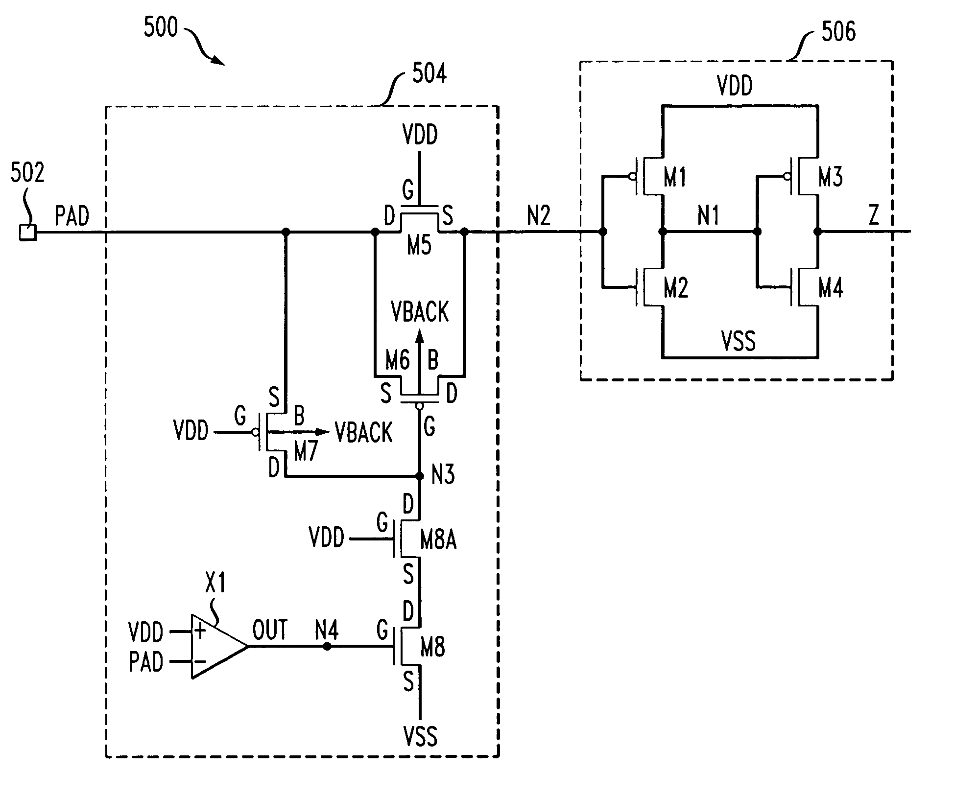
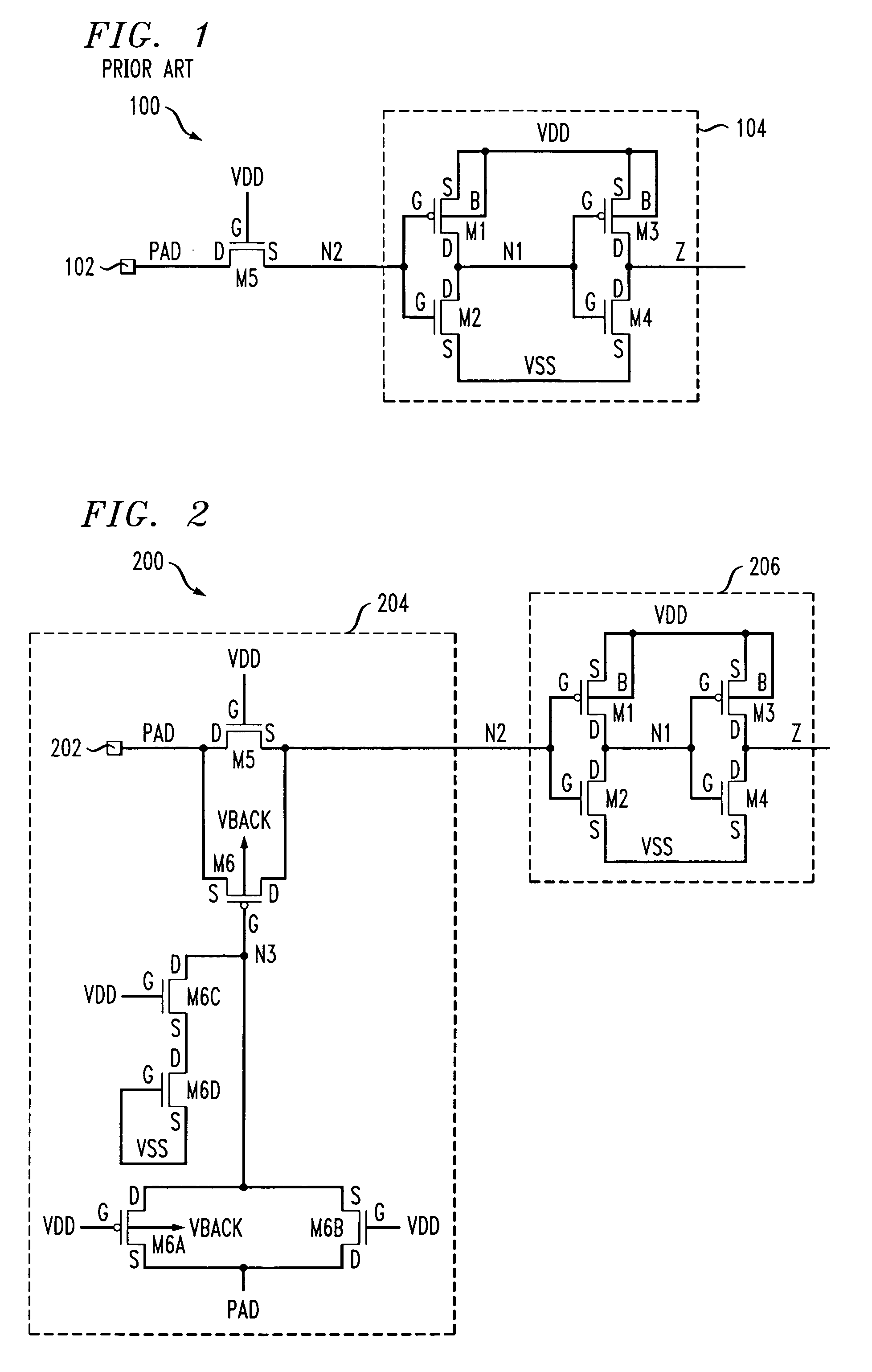
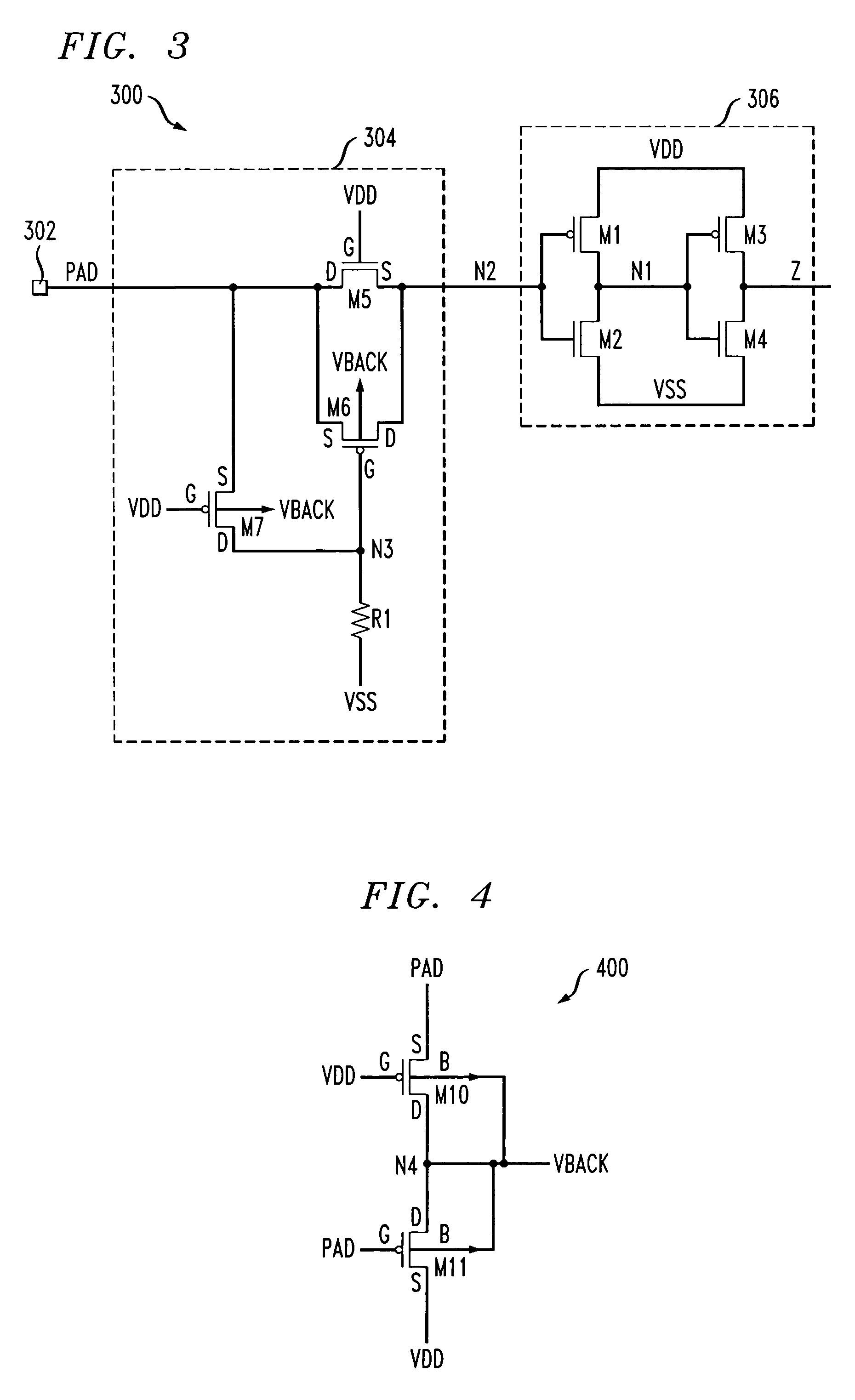
[0016]The present invention will be described herein in the context of illustrative buffer circuits. It should be understood, however, that the present invention is not limited to these or any other particular circuit arrangements. Rather, the invention is more generally applicable to techniques for providing overvoltage protection to a buffer circuit, without significantly reducing a speed and / or input voltage swing of the buffer circuit. Although implementations of the present invention are described herein with specific reference to PMOS and NMOS transistor devices, as may be formed using a CMOS fabrication process, it is to be understood that the invention is not limited to such transistor devices and / or such a fabrication process, and that other suitable devices, such as, for example, bipolar junction transistors (BJTs), etc., and / or fabrication processes (e.g., bipolar, BiCMOS, etc.), may be similarly employed, as will be apparent to those skilled in the art.

[0017]FIG. 1 is a ...


PUM


Abstract

A buffer circuit having enhanced overvoltage protection includes core buffer circuitry couplable to a first voltage source having a first voltage level. The core buffer circuitry is configured to receive a first signal and to generate a second signal which is a function of the first signal. The buffer circuit further includes a protection circuit coupled between the core buffer circuitry and a signal pad. The protection circuit is operative: (i) to clamp the first signal to about the first voltage level when a third signal received at the signal pad exceeds the first voltage level by a first amount; and (ii) to generate the first signal being substantially equal to the third signal when the third signal is less than or substantially equal to the first voltage level.

Description

FIELD OF THE INVENTION[0001]The present invention relates generally to electronic circuits, and more particularly relates to buffer circuits with overvoltage protection.BACKGROUND OF THE INVENTION[0002]Buffer circuits (e.g., output buffers, input buffers and bidirectional buffers) are employed in a variety of electronic devices and applications. In certain applications, a buffer circuit may be subjected to a voltage potential that is substantially higher than that which is supported by the specific process technology used to fabricate the buffer circuit. For example, a buffer circuit fabricated using a 3.3 volt (V) process may be subjected to a 5.0V input signal. In order to avoid over-stressing the devices in the buffer circuit, an N-channel metal-oxide-semiconductor (NMOS) protection device, M5, gated by a supply voltage VDD of the buffer circuit 100, may be placed in series between an input pad (PAD) 102 and the remainder 104 of the buffer circuitry, as shown in FIG. 1. The inclu...

Claims


Application Information

Patent Timeline
Patent Type & Authority Patents(United States)
IPC IPC(8): H02H3/20
CPCH03K19/00315H03K2217/0018
Inventor BHATTACHARYA, DIPANKARKOTHANDARAMAN, MAKESHWARKRIZ, JOHN C.MORRIS, BERNARD L.
Owner AVAGO TECH INT SALES PTE LTD
Why Eureka
Try Eureka