Posted precharge and multiple open-page RAM architecture

a pre-charge operation and open-page technology, applied in the field of electronic systems, can solve the problems of unproductive latencies, waste of clock cycles, and inability to allow row accesses of less than a burst length of 4, and achieve the effect of reducing the execution time of the pre-charge operation

Inactive Publication Date: 2008-10-07
DATASECURE
View PDF10 Cites 53 Cited by
  • Summary
  • Abstract
  • Description
  • Claims
  • Application Information

AI Technical Summary

Benefits of technology

[0017]The present invention provides a method and architecture that overcomes the problem of latency-caused performance degradation discussed above. The invention involves the use of what is termed herein a “Posted Precharge,” which as used herein means that an external command for Precharge is given as early as possible, preferably immediately following a Read command. However, the present invention causes the execution of the Precharge to be delayed by means of an internal mechanism, preferably a counter means, until all Read / Write commands are completed. According to a preferred aspect of the invention, the method and architecture also provide that any subsequent access to the same page causes the counter means to be reset, further delaying the execution of the Precharge operation. In other words, the invention provides an internal Precharge scheme that starts the Precharge for that particular bank, activity-dependent, at an appropriate time, thus freeing up the command bus.
[0019]The benefits of this invention can be promoted by implementing the Posted Precharge on the DDR device itself, which has the potential for virtually eliminating command bus contentions. The benefits of Posted Precharge can also be obtained in DIMM's and SIMM's (and similar memory modules and / or subsystems) by implementing some or all of the features of the invention described herein in the memory controller (which manages memory module access and proper operation).
[0020]As noted above, the DDR-II does not provide for a 4 bit burst intra-burst interruption, and the minimum unit of data that can be efficiently accessed is 4 bits times the number of I / O pins. Thus in the case of shorter accesses, such as are required for networking operations and other applications, only a fraction of the bursted data is required at the processor level, and the balance represents wasted clock cycles and unproductive latencies. Further, the emerging hyperthreading, multithreading, multichannel-DRAM access, shared memory and other processor inventions referred to above are making multiple open-page capability in every bank an essential capability for the future, without incurring the latencies that currently attend intra-bank, multi-row accesses. In addition, the posted precharge allows the re-accessing of a previous page without incurring worst case scenario latencies.

Problems solved by technology

Notably, the DDR-II architecture does not allow row accesses of less than a burst length of 4.
Thus in the case of shorter accesses, such as are required for networking operations and other applications, only a fraction of the bursted data is required at the processor level, and the balance represents wasted clock cycles and unproductive latencies.

Method used


Image

  • Posted precharge and multiple open-page RAM architecture
  • Posted precharge and multiple open-page RAM architecture
  • Posted precharge and multiple open-page RAM architecture

Examples


Embodiment Construction

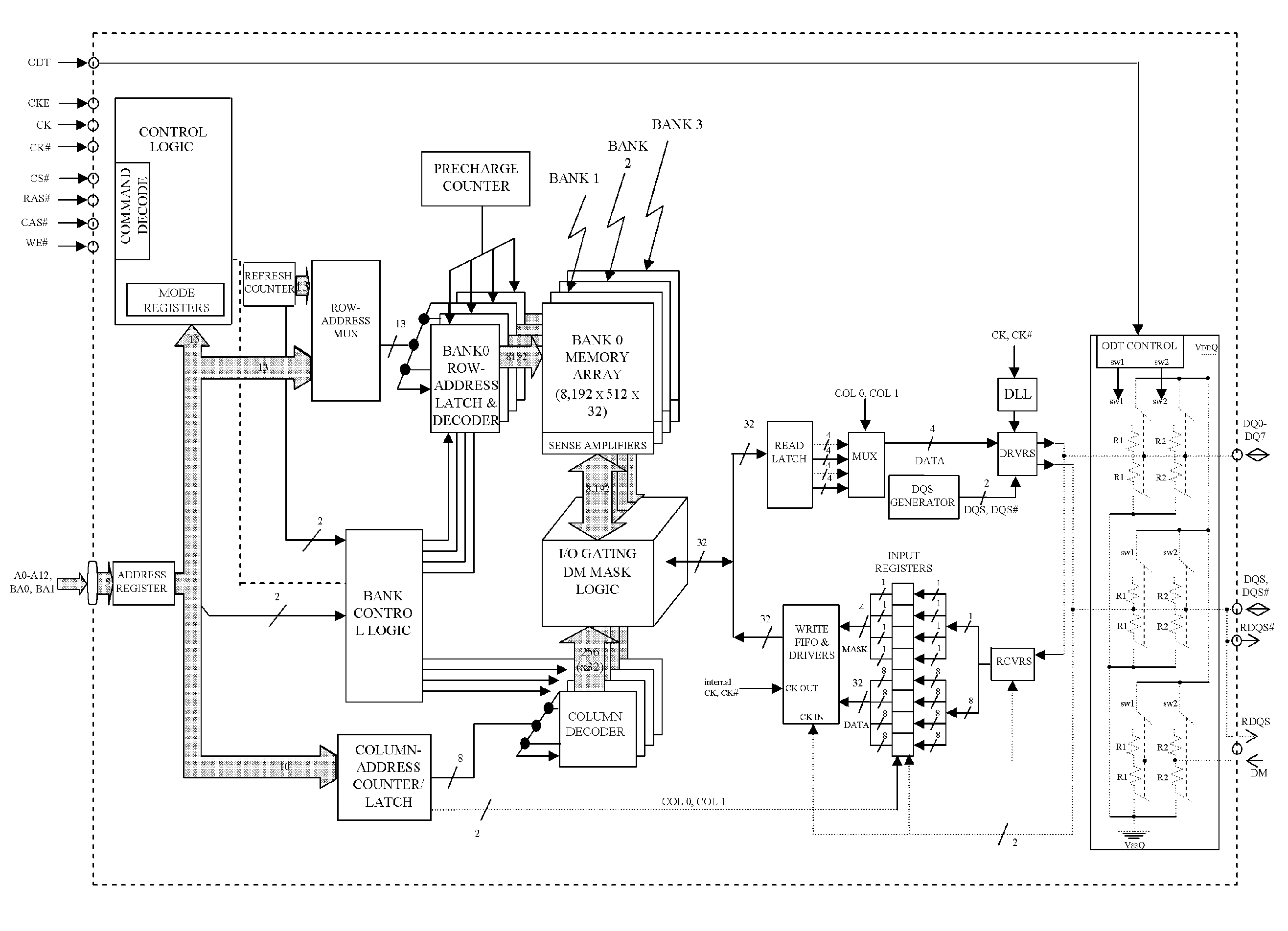
[0035]The utilization of the present invention applies to volatile as well as nonvolatile memories. Implementation in stand alone memory devices, SOC (System On Chip), SIP (System In Package), SIC (System In Chip), DIMM's (Dual In Line Memory Modules), SIMM's (Single In Line Memory Modules) and other combinations are possible. Furthermore, “page” architecture is widely used in DRAM's and flash memories, the operations of the latter being described in detail in the available literature and therefore will not be discussed in any detail here. “Precharge” is widely used for dynamic devices like DRAM's, FeRAM's (ferroelectric RAM's), etc. “Page” architecture is also expected to influence future memory products like MAG RAM's, plastic RAM's, CNT RAM's (carbon nano tube), organic memories, phase-change memories, molecular memories and similar products. As such, the implementation of the present invention encompasses all such devices, as well as other memory devices that employ a page archi...


PUM


Abstract

A method and architecture that overcomes the problem of latency-caused performance degradation of electronic memory systems. The method involves a “Posted Precharge,” by which an external command for Precharge is given as early as possible, such as immediately following a Read command. The execution of the Precharge is delayed by a precharge counter until all Read / Write commands are completed. By posting a precharge command on a bus at the first available opportunity, multiple pages can be open on the same bank of a memory device. As a result, access latencies are significantly reduced and efficiency of bus in electronic memory systems is significantly improved.

Description

CROSS REFERENCE TO RELATED APPLICATIONS[0001]This application claims the benefit of U.S. Provisional Application Nos. 60 / 510,182 filed Oct. 10, 2003, and 60 / 525,453, filed Nov. 28, 2003.BACKGROUND OF THE INVENTION[0002]The present invention generally relates to electronic systems utilizing memory devices. More particularly, this invention relates to a method and memory architecture that enables multiple pages to be open on the same bank of a memory device.[0003]High density random access memories (RAM) find numerous applications in computers, communications, and consumer and industrial applications. These memories are mostly volatile (lose stored data when power is switched off). These cost sensitive, medium performance (high bandwidth with moderate latency) segments have been served by multibank SDRAM's (synchronous dynamic random access memories). SDR SDRAM's, DDR-I SDRAM's, DDR-II SDRAM's, QDR SDRAM's, Rambus™ DRAM's, Network DRAM's™, FCRAM's™, and RLDRAM's™ are among the numerou...

Claims


Application Information

Patent Timeline
Patent Type & Authority Patents(United States)
IPC IPC(8): G11C8/00G11C11/00G11C11/4076G11C11/4094
CPCG11C11/4076G11C11/4094
Inventor RAO, G. R. MOHANSCHUETTE, FRANZ MICHAEL
Owner DATASECURE
Why Eureka
Try Eureka