Probe skates for electrical testing of convex pad topologies

a convex pad and topology technology, applied in the direction of electrical testing, measurement devices, instruments, etc., can solve the problems of unusable wafers, unfavorable convex pad topology testing, and non-conductive layer of debris on the pad, so as to improve the tolerance of overdrive motion, prolong the mean time, and improve the control of the skate

Active Publication Date: 2008-10-14
MICRO PROBE
View PDF2 Cites 25 Cited by
  • Summary
  • Abstract
  • Description
  • Claims
  • Application Information

AI Technical Summary

Benefits of technology

[0014]One aspect of the present invention is a method of using the self-cleaning skate by providing a conductive pad having a generally convex shape and a non-conductive layer of debris, such as a granular non-conductive oxidation surface, and providing a conductive probe for engaging the conductive pad. The probe includes a contact end for receiving a test current, a retention portion below the contact end, a block for holding the retention portion, a probe arm below the retention portion, a probe contact tip below the arm, and a generally planar self-cleaning skate disposed perpendicular below the contact tip, where the skate has a generally square front end, a generally round back end and a generally flat middle section therebetween. The skate is positioned above the conductive pad, where the conductive pad is translated, causing the skate to engage the conductive pad. Overdrive motion is then provided to the conductive pad causing the skate to scrub the debris from the conductive pad and clean the debris from the region of the skate that contacts the conductive pad. The cleaning occurs from the overdrive motion moving the skate to form an angle between the skate middle section and a horizontal plane, while engaging the round back end with the conductive pad. The overdrive motion induces a translation motion of the skate back end along the pad in a direction towards the skate front end while the skate middle section is further angled with respect to the horizontal plane. As the skate back end translates across the conductive pad, debris and non-conductive oxides are displaced along the skate, where the debris moves around the round back end to a position on the skate that is away from the conductive pad. Reversing the overdrive motion to the pad causes the skate middle section to move from the angle to approximately the horizontal position, where the skate flat middle section is in contact with the conductive pad. Here, the debris on the skate back end moves to a position away from the conductive pad. Continuing to reverse the overdrive motion translates the skate along the horizontal position and further moving the debris around the round back end to a position on the skate that is away from the conductive pad. Finally, the pad is translated to cause the probe to disengage from the conductive pad. The method according to the current invention improves overdrive control by making the scrubbing and cleaning less sensitive to the overdrive motion, where the debris layer is removed without breaching or damaging the conductive pad and debris is displaced from the conductive pad to the skate. Further, a current (i) is applied to the probe after the self-cleaning skate contacts the conductive pad. Using the self-cleaning skate according to the invention is accomplished after at least two engagement cycles.
[0017]Some key advantages of the invention are the features of the self-cleaning skate extend the mean time between failure of the probe caused by debris buildup on the skate. Additionally, due to the unique skate design, a scrub channel may be made on irregularly shaped conductive pads at any location on the pad. The current invention provides better control of the skate during overdrive motion, where improved tolerance to overdrive motion enables reliable pad testing on silicon wafers before dicing.

Problems solved by technology

A problem exists with a non-conductive layer of debris on the pad such as a non-conductive oxide layer impeding the conductive pad from receiving the test signal, where the debris is an artifact of the fabrication process.
Numerous problems arise from this method such as controlling the probe scrubbing action, managing undesirable debris accumulation on the probe tip, and the added need for a complicated and invasive probe cleaning processes to remove the debris from the probe tips.
A probe is often too sensitive to the overdrive motion from the pad, causing a scrub depth that is too deep that not only removes a portion of the non-conductive layer, but also damages or breaches the conductive pad, thus rendering the wafer unusable.
Debris accumulation on the probe tip degrades the electrical continuity between the probe and conductive pad, often times restricting the test signal and providing erroneous test results, where implementation of an undesirable test redundancy may then become necessary.
Such a technique not only disrupts the fabrication throughput, but also degrades the probe tip, resulting in shortened utility of the probes and requiring premature replacement.
While such an alloy lends itself for creating a tip that is more robust for scrubbing, the need to disrupt fabrication throughput for a probe tip cleaning process still exists.
Further, the geometry of the contact bump made from the alloy nub lends itself for undesirable accumulation of debris, thus necessitating relatively frequent cleaning.
Unfortunately, such geometry has been shown to lack scrubbing control and damage the pad due to the probe having a hyper-sensitivity to overdrive motion.

Method used


Image

  • Probe skates for electrical testing of convex pad topologies
  • Probe skates for electrical testing of convex pad topologies
  • Probe skates for electrical testing of convex pad topologies

Examples


Embodiment Construction

[0029]Although the following detailed description contains many specifics for the purposes of illustration, anyone of ordinary skill in the art will readily appreciate that many variations and alterations to the following exemplary details are within the scope of the invention. Accordingly, the following preferred embodiment of the invention is set forth without any loss of generality to, and without imposing limitations upon, the claimed invention.

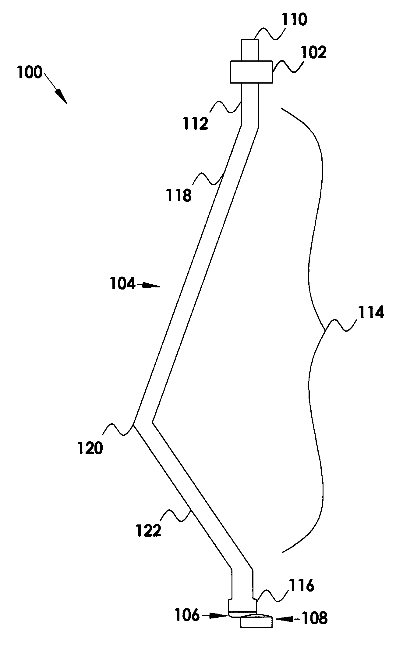
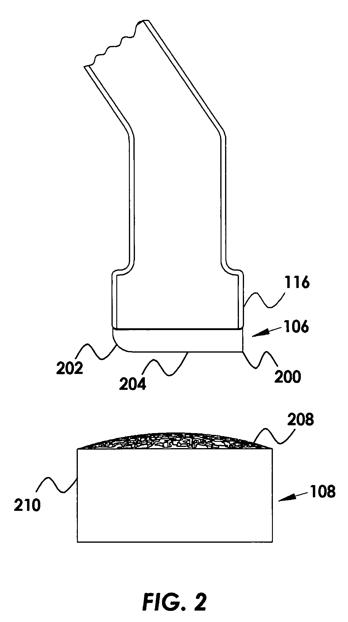
[0030]Semiconductor wafer processing methods and technology have been dynamic fields and continue to be the focus of much research and development. Among the numerous areas of these fields, early verification of process integrity and circuit design is an important step for effective cost control and manufacturing efficiency. As new methods of fabrication and new semiconductor wafer features evolve, testing methods must adapt to these changes. For example, the conductive pad of a semiconductor wafer can be fabricated as a dome-shape, or ev...


PUM


Abstract

A probe for engaging a conductive pad is provided. The probe includes a probe contact end for receiving a test current, a probe retention portion below the contact end, a block for holding the probe retention portion, a probe arm below the retention portion, a probe contact tip below the arm, and a generally planar self-cleaning skate disposed perpendicular below the contact tip. The self-cleaning skate has a square front, a round back and a flat middle section. The conductive pad is of generally convex shape having a granular non-conductive surface of debris and moves to engage the skate, whereby an overdrive motion is applied to the pad causing the skate to move across and scrub non-conductive debris from the pad displacing the debris along the skate and around the skate round back end to a position on the skate that is away from the pad.

Description

CROSS-REFERENCE TO RELATED APPLICATIONS[0001]This application is a continuation-in-part application of the inventor's prior U.S. application Ser. No. 11 / 480,302 filed Jun. 29, 2006, for PROBES WITH SELF-CLEANING SKATES FOR CONTACTING CONDUCTIVE PADS, which claims the benefit of U.S. application Ser. No. 10 / 850,921 filed on May 21, 2004, now U.S. Pat. No. 7,148,709, U.S. application Ser. No. 10 / 888,347 filed on Jul. 9, 2004 and U.S. application Ser. No. 11 / 450,977 filed on Jun. 9, 2006.FIELD OF THE INVENTION[0002]The invention relates generally to an apparatus and method of using contacting tips of probes in scrubbing and electrical testing of a device under test. More particularly, the invention relates to an apparatus and method of using contacting tips having probe skates with geometries that provide self-cleaning and a reduction in sensitivity to overdrive motion.BACKGROUND[0003]Semiconductor wafer testing before dicing is a necessary and critical process step. Such testing provi...

Claims


Application Information

Patent Timeline
Patent Type & Authority Patents(United States)
IPC IPC(8): G01R31/02
CPCG01R1/06733G01R3/00
Inventor KISTER, JANUARY
Owner MICRO PROBE
Why Eureka
Try Eureka