Solid state imaging device

a solid-state imaging and imaging device technology, applied in the field of solid-state imaging devices, can solve the problems of inadequate countermeasures and unintentional state imaging devices, and achieve the effect of reducing optical noise and not reducing light receiving efficiency

Inactive Publication Date: 2008-11-04
FUJIFILM CORP
View PDF9 Cites 11 Cited by
  • Summary
  • Abstract
  • Description
  • Claims
  • Application Information

AI Technical Summary

Benefits of technology

[0005]In view of the foregoing, an object of the present invention is to provide a solid state imaging device which effectively reduces noises caused by oblique incident light.
[0010]According to the solid state imaging device of the present invention, the light diffusion layer or the light absorbing layer is formed in the recesses to diffuse or absorb the incident light oblique to the optical axis of the optical lens. Therefore, the optical noise is reduced effectively.
[0011]In addition, the light diffusion layer or the light absorbing layer is disposed outside the optical path of the incident light substantially parallel to the optical axis of the optical lens, and therefore light receiving efficiency is not decreased.

Problems solved by technology

However, this solid state imaging device does not aim to prevent the incoming of the light under the light shielding layer, and is still not an adequate countermeasure.

Method used


Image

  • Solid state imaging device
  • Solid state imaging device
  • Solid state imaging device

Examples


Embodiment Construction

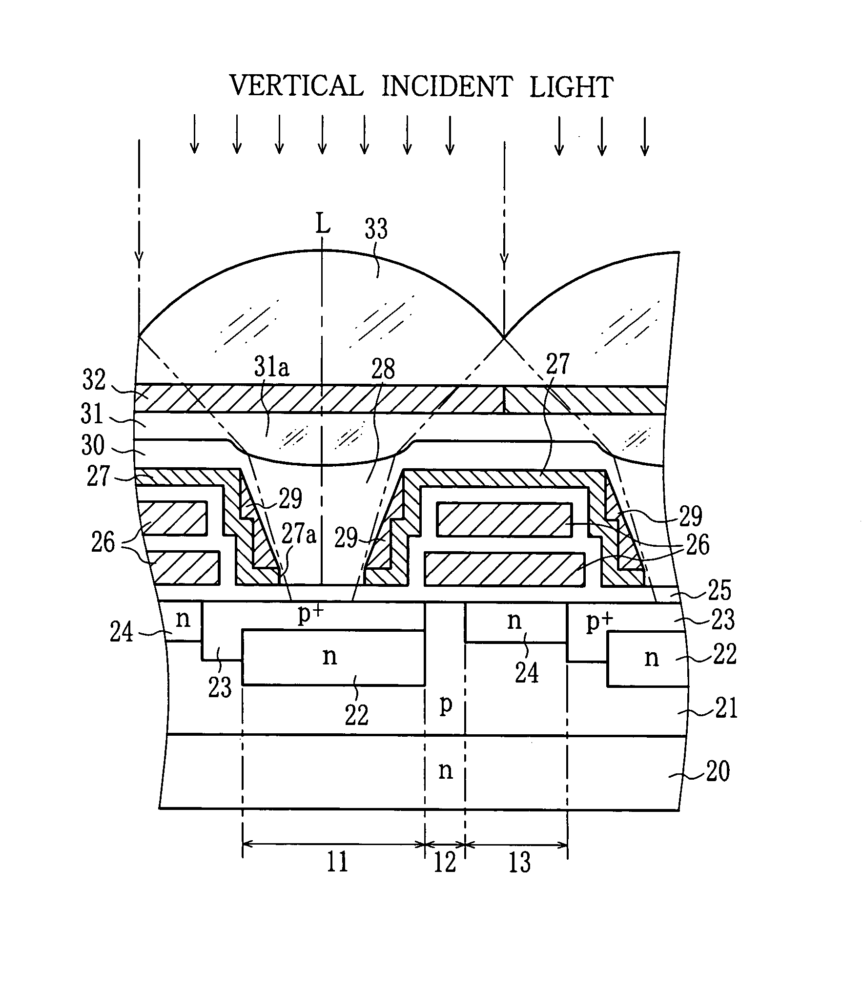
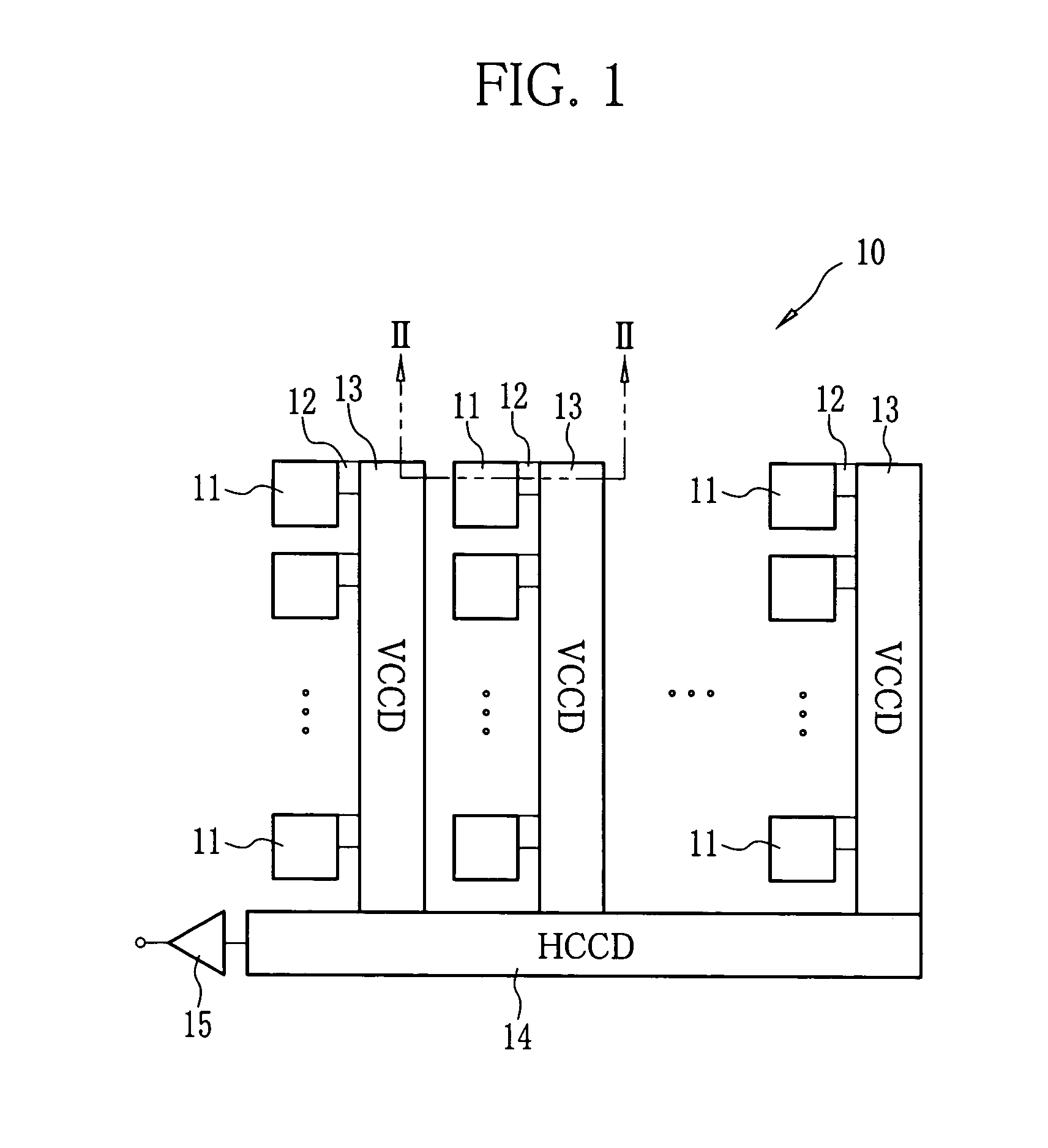
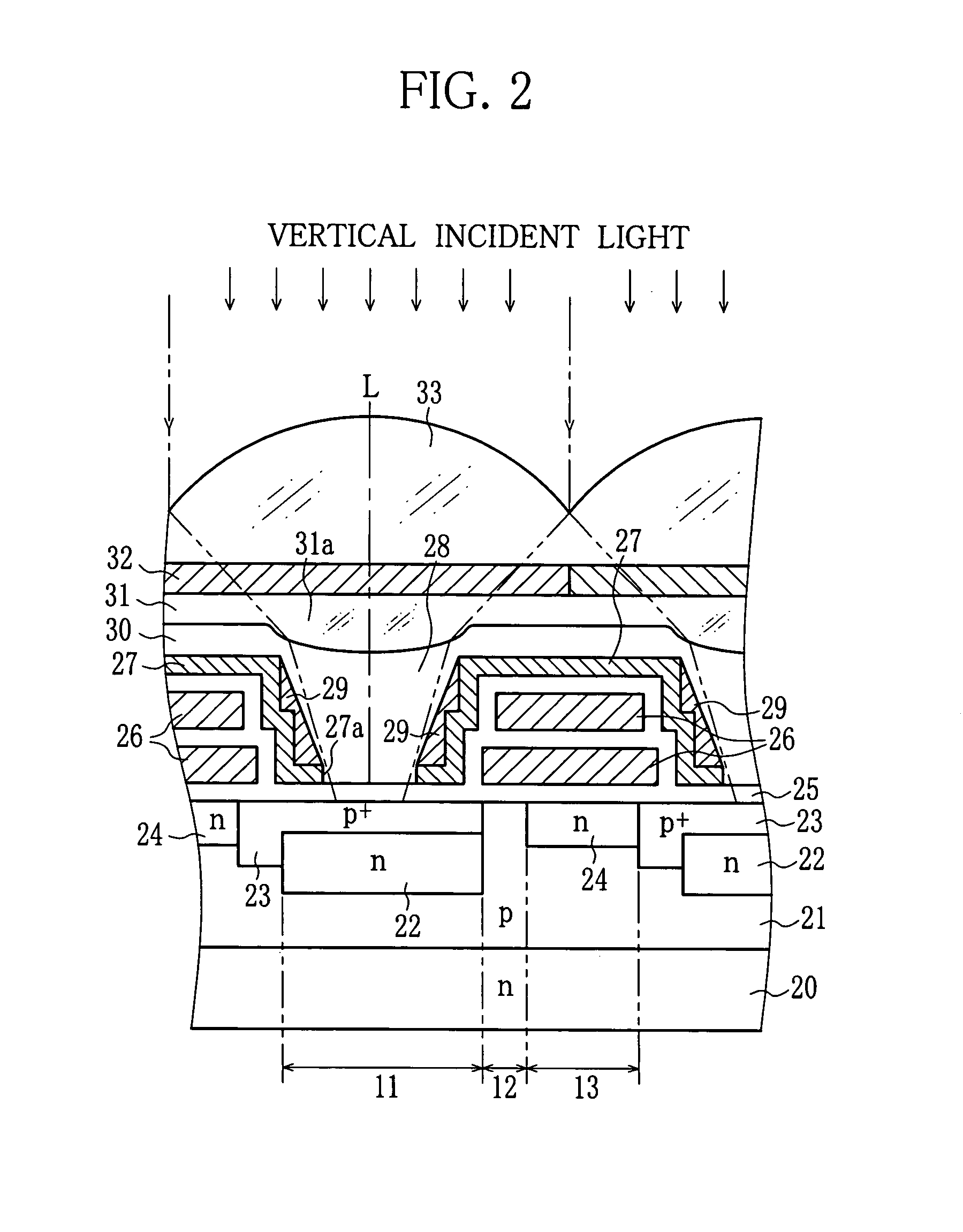
[0018]As shown in FIG. 1, a CCD image sensor 10 has a plurality of photodiodes 11 in a two-dimensional matrix arrangement, readout transfer gates 12 provided for each of the photodiodes 11, vertical CCDs 13 provided for each column of the photodiodes 11, a horizontal CCD 14 connected to a terminal end of every vertical CCD 13, and an output amplifier 15 connected to a terminal end of the horizontal CCD 14.

[0019]Each photodiode 11 photoelectrically converts incident light into signal charge and stores it. After the exposure time is passed, the readout transfer gates 12 turn into an open state to allow the signal charge stored in the photodiodes 11 to move to the vertical CCDs 13. The vertical CCDs 13 send the signal charge, coming from the photodiodes 11 through the readout transfer gates 12, to the horizontal CCD 14 in a stepwise manner. The horizontal CCD 14 receives the signal charge from the vertical CCDs 13 step by step sequentially, and sends it in a horizontal direction toward...


PUM


Abstract

A CCD image sensor includes photodiodes, vertical transfer CCDs for transferal of signal charge of the photodiodes, and a light shielding layer for protection of the vertical transfer CCDs from light. The light shielding layer covers over recesses disposed above the photodiodes, and each of the recesses has an opening on the bottom to expose a light receiving surface of the photodiode. A light diffusion layer is formed on the light shielding layer in each recess. Since the incident light oblique to an optical axis of a microlens is diffused by the light diffusion layer, the vertical CCDs hardly receive the light coming from around the edges of the opening.

Description

FIELD OF THE INVENTION[0001]The present invention relates to solid state imaging devices such as CCD image sensors, and more particularly to solid state imaging devices capable of preventing optical noises.BACKGROUND OF THE INVENTION[0002]In solid state imaging devices such as CCD image sensors, an optical noise called smear is sometimes produced. The smear is induced by unwanted electric charge in a vertical CCD, and such unwanted electric charge arises from intense light which enters the solid state imaging device at an oblique angle. As shown in FIG. 5, the incident light at an oblique angle from an optical axis L of a microlens 33 is reflected on a recess of a light shielding layer 27. The reflected light goes under the light shielding layer 27 from an opening 27a of the light shielding layer 27 to penetrate an insulation layer 25, and finally encounters a vertical CCD 13. This incident light to the vertical CCD 13 undergoes the photoelectric conversion, and produces the unwante...

Claims


Application Information

Patent Timeline
Patent Type & Authority Patents(United States)
IPC IPC(8): H01L31/062H01L27/14H01L27/146H04N5/335H04N5/359H04N5/369
CPCH01L27/14623H01L27/14806H01L27/14627
Inventor MISAWA, TAKESHI
Owner FUJIFILM CORP
Why Eureka
Try Eureka