Composite hard bias design with a soft magnetic underlayer for sensor applications

a soft magnetic underlayer and sensor technology, applied in nanoinformatics, instruments, record information storage, etc., can solve the problems of reducing the biasing strength and efficiency, undesirably high magnetostriction, and the method for fabricating this device appears to be complicated and expensive, so as to reduce the length of the biasing dispersion

Active Publication Date: 2008-11-04
HEADWAY TECH INC
View PDF24 Cites 32 Cited by
  • Summary
  • Abstract
  • Description
  • Claims
  • Application Information

AI Technical Summary

Benefits of technology

[0021]One objective of the present invention is to provide a hard bias structure in which the longitudinal biasing dispersions are reduced at an abutting junction with a free layer in a magnetoresistive (MR) element.
[0022]A further objective of the present invention is to provide a hard bias structure for biasing a free layer in a GMR sensor device that improves the output signal, asymmetry sigma, and head noise (edge domain noise, etc.) which is measured by the normalized base line wandering (NBLW) reject rate.
[0026]In a second embodiment, the magnetic read head includes the same layers as in the first embodiment except that the hard bias structure is laminated such that the magnetic underlayer / hard bias layer configuration is repeated a plurality of times on the seed layer. Thus, the hard bias structure may be represented by [magnetic underlayer / hard bias layer]n where n is an integer ≧2. The thickness of the individual layers may be adjusted so that the hard bias structure has optimum HC and Mrt values and provides a stable longitudinal bias to an adjacent free layer in the GMR element.
[0028]Alternatively, the hard bias structure may be laminated in which the soft magnetic underlayer / hard bias layer configuration is repeated a plurality of times to form a plurality of stacks represented by [magnetic underlayer / hard bias layer]n on the seed layer. The thicknesses of the individual layers within the hard bias structure are adjusted to reduce dispersions, provide optimum HC and Mrt values, and minimize the asymmetry sigma in the output signal during a read operation.

Problems solved by technology

Thus, the biasing direction will become randomized along the junction edge and thereby decrease the biasing strength and efficiency.
Unfortunately, the high magnetic saturation of FeCo alloys generally leads to undesirably high magnetostriction.
However, the method for fabricating this device appears to be complicated and expensive.

Method used


Image

  • Composite hard bias design with a soft magnetic underlayer for sensor applications
  • Composite hard bias design with a soft magnetic underlayer for sensor applications
  • Composite hard bias design with a soft magnetic underlayer for sensor applications

Examples


second embodiment

[0035]The present invention is an improved hard bias structure in a magnetic read head that reduces dispersions of biasing strength along a junction edge with a free layer in a magnetoresistive (MR) element. Although the exemplary embodiments depict a CIP spin valve for a GMR sensor device, those skilled in the art will appreciate that the present invention may also apply to CPP spin valves, magnetic tunnel junction (MTJ) devices, or to multilayer sensor designs based on a GMR or SVMR effect. The drawings are provided by way of example and are not intended to limit the scope of the invention. For example, the shape of a MR element in a magnetic device is not a limitation and the present invention encompasses any configuration where a hard bias structure as described in the first or second embodiment forms an abutting junction with a free layer in the MR element. Moreover, the MR element may be comprised of either a top spin valve or a bottom spin valve. The present invention is also...

first embodiment

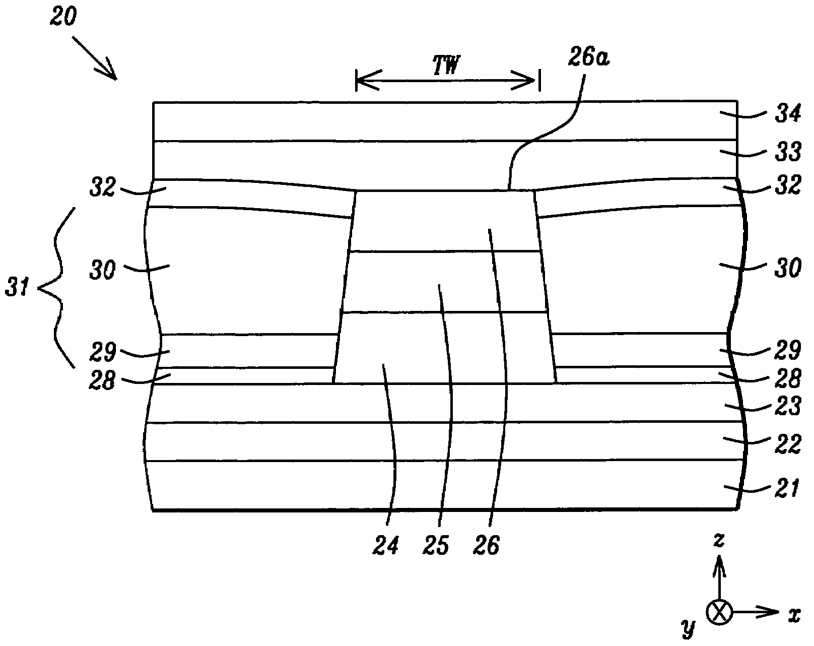
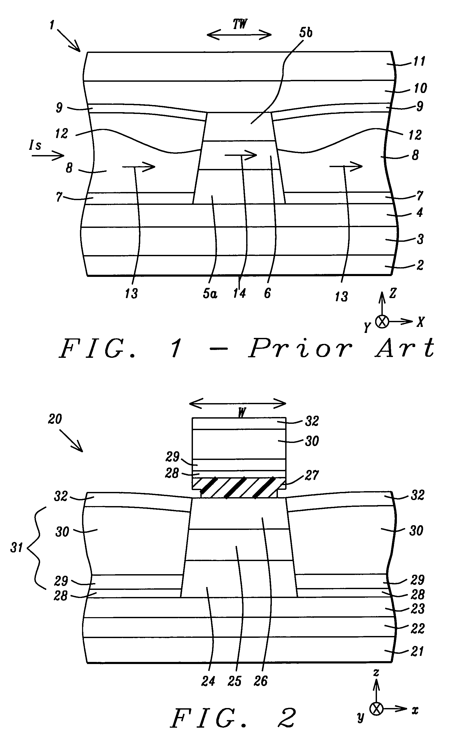
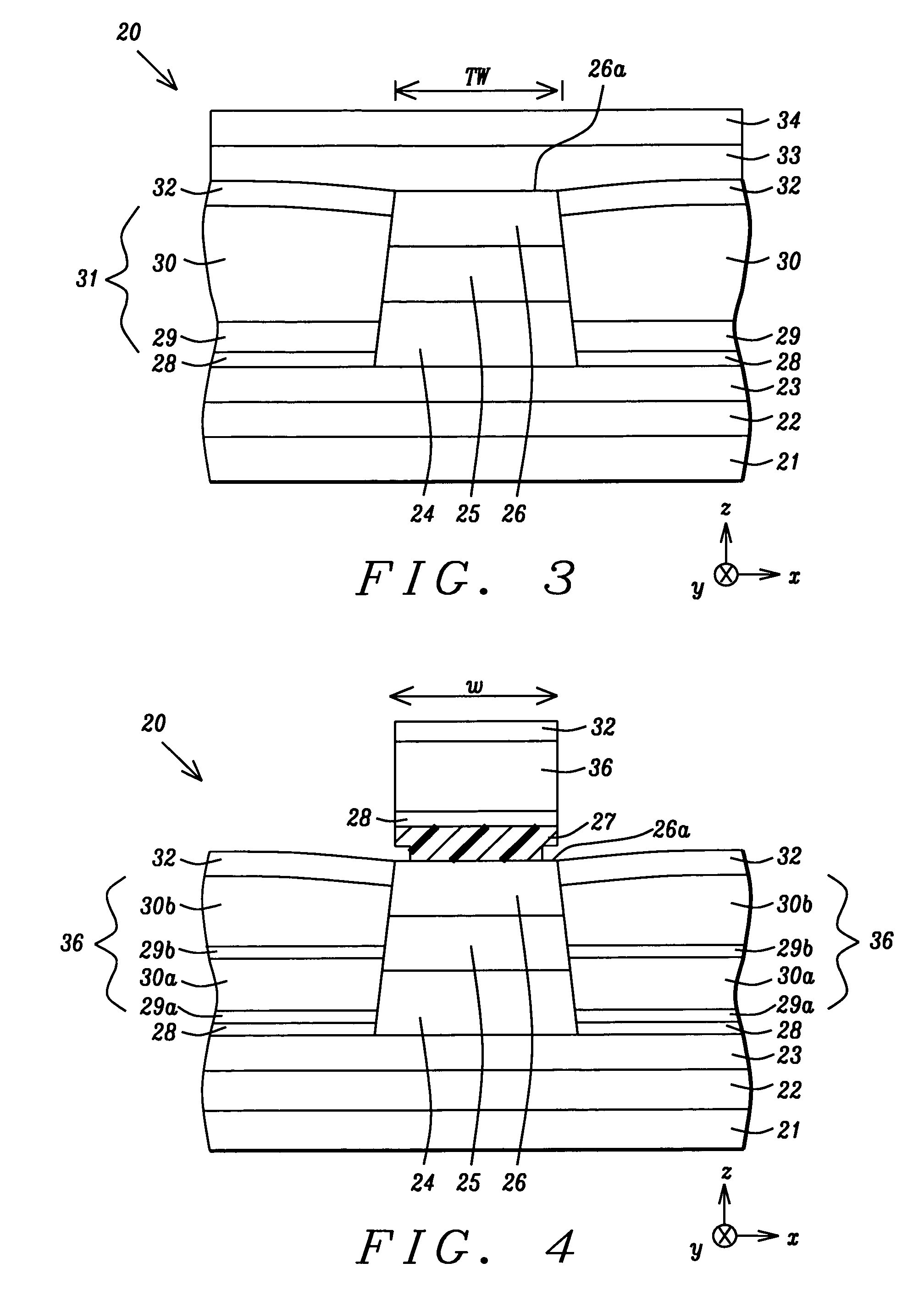
[0036]A first embodiment is depicted in FIGS. 2-3. Referring to FIG. 2, a cross-sectional view from an ABS plane is shown of a partially completed magnetic read head 20 formed on a substrate 21 that may be a ceramic layer, for example. A first shield layer 22 is formed on the substrate 21 and a first gap layer 23 is formed on the first shield layer by a conventional method. There is a GMR sensor element which is a stack comprised of a bottom portion 24, a free layer 25, and a top portion 26 sequentially formed on the first gap layer 23. The GMR sensor element typically has sloped sidewalls wherein the top portion 26 has a smaller width than the bottom portion 24.

[0037]The GMR sensor element is fabricated by sequentially depositing a stack of layers that comprises a bottom portion 24, a free layer 25, and a top portion 26 by an argon sputtering technique, for example, which is well known in the art. A photoresist layer 27 having a width w is patterned on the top portion 26 and then a...


PUM

PropertyMeasurementUnit
coercivityaaaaaaaaaa
thicknessaaaaaaaaaa
thicknessaaaaaaaaaa

Abstract

A hard bias structure for biasing a free layer in a MR element within a magnetic read head is comprised of a soft magnetic underlayer such as NiFe and a hard bias layer comprised of Co78.6Cr5.2Pt16.2 or Co65Cr15Pt20 that are rigidly exchange coupled to ensure a well aligned longitudinal biasing direction with minimal dispersions. The hard bias structure is formed on a BCC seed layer such as CrTi to improve lattice matching. The hard bias structure may be laminated in which each of the underlayers and hard bias layers has a thickness that is adjusted to optimize the total Hc, Mrt, and S values. The present invention encompasses CIP and CPP spin values, MTJ devices, and multi-layer sensors. A larger process window for fabricating the hard bias structure is realized and lower asymmetry output and NBLW (normalized base line wandering) reject rates during a read operation are achieved.

Description

[0001]This application is related to U.S. patent application Ser. No. 11 / 016,506 and filed Dec. 17, 2004, owned by a common assignee as the instant invention.RELATED PATENT APPLICATION[0002]This application is related to the following: Ser. No. 10 / 868,716, filing date Jun. 15, 2004; and Ser. No. 11 / 016506, filing date Dec. 17,2004; all assigned to a common assignee.FIELD OF THE INVENTION[0003]The invention relates to an improved hard bias structure formed adjacent to a giant magnetoresistive (GMR) sensor in a magnetic read head and a method for making the same. In particular, a soft magnetic underlayer is coupled with an adjoining hard bias layer to reduce biasing dispersions at an abutting junction with a free layer and improve the output signal and asymmetry sigma in a read operation.BACKGROUND OF THE INVENTION[0004]In a magnetic recording device in which a read head is based on a spin valve magnetoresistance (SVMR) or a giant magnetoresistance (GMR) effect, there is a constant dr...

Claims


Application Information

Patent Timeline
Patent Type & Authority Patents(United States)
IPC IPC(8): G11B5/33G11B5/127
CPCB82Y10/00B82Y25/00G11B5/3909G11B5/3932G11B2005/3996
Inventor ZHANG, KUNLIANGCHEN, MAO-MINTORNG, CHYU-JIUHLI, MINCHIEN, CHEN-JUNG
Owner HEADWAY TECH INC
Why Eureka
Try Eureka