Semiconductor device and method of manufacturing the same

a technology of semiconductor devices and semiconductor films, which is applied in the direction of semiconductor devices, electrical devices, transistors, etc., can solve the problems of difficult to obtain good characteristics of semiconductor devices and inability to obtain excellent gate insulating films, etc., and achieves excellent characteristics, no increase in interface states, and uniform thickness

Active Publication Date: 2008-11-11
TOKYO ELECTRON LIMITED ONE HALF 50 OF ALL RIGHT TITLE & INTEREST +1
View PDF15 Cites 1 Cited by
  • Summary
  • Abstract
  • Description
  • Claims
  • Application Information

AI Technical Summary

Benefits of technology

[0006]According to this invention, a gate insulating film is formed using a plasma on a silicon substrate surface having a three-dimensional structure with a plurality of crystal orientations. The plasma gate insulating film exhibits no increase in interface state in any crystal orientations and has a uniform thickness even at corner portions of the three-dimensional structure. By forming the high-quality gate insulating film using the plasma, there is obtained a semiconductor device having excellent characteristics.

Problems solved by technology

However, when the gate insulating film is formed on the substrate surface by thermal treatment in the semiconductor device of the double-gate structure or the triple-gate structure, the interface states between silicon and the insulating film (Si / SiO2) increase other than in a (100) crystal orientation to degrade the quality of the oxide film and, therefore, it has been difficult to obtain good characteristics as the semiconductor device.
Further, there is a problem that the insulating film cannot be formed uniform at edge portions of the three-dimensional structure, and so on, so that an excellent gate insulating film cannot be obtained.

Method used


Image

  • Semiconductor device and method of manufacturing the same
  • Semiconductor device and method of manufacturing the same
  • Semiconductor device and method of manufacturing the same

Examples


first embodiment

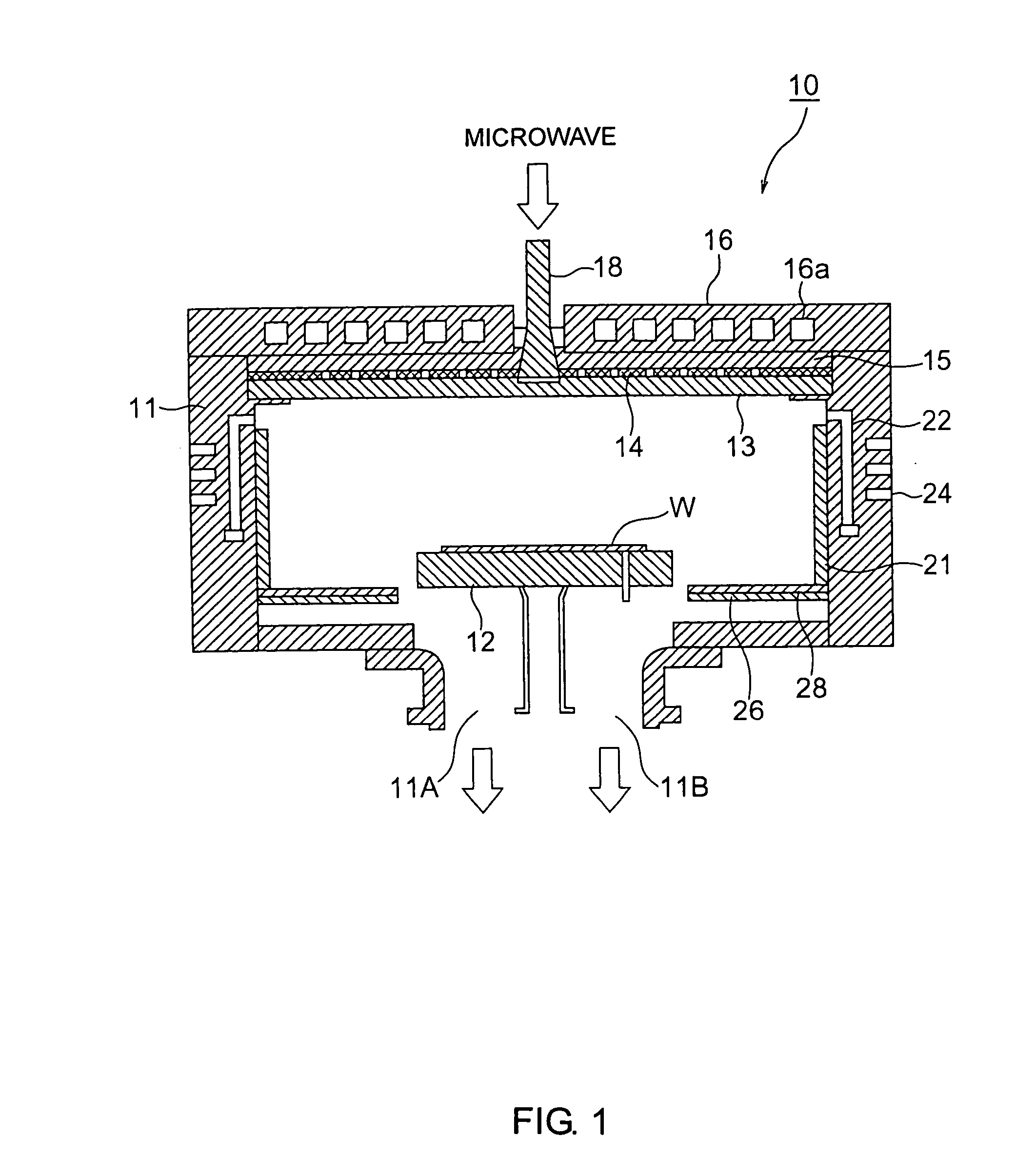
[0010]FIG. 1 shows an example of a schematic structure of a plasma processing apparatus 10 used in this invention. The plasma processing apparatus 10 has a processing container 11 provided with a substrate holding stage 12 for holding a silicon wafer W as a substrate to be processed. Gas within the processing container 11 is exhausted from exhaust ports 11A and 11B through a non-illustrated exhaust pump. The substrate holding stage 12 has a heater function for heating the silicon wafer W. A gas baffle plate (partition plate) 26 made of aluminum is disposed around the substrate holding stage 12. A quartz cover 28 is provided on an upper surface of the gas baffle plate 26.

[0011]The processing container 11 is provided, in the apparatus upper part thereof, with an opening portion corresponding to the silicon wafer W on the substrate holding stage 12. This opening portion is closed by a dielectric plate 13 made of quartz or Al2O3. A planar antenna 14 is disposed on the upper side of the ...


PUM


Abstract

A gate insulating film is formed using a plasma on a three-dimensional silicon substrate surface having a plurality of crystal orientations. The plasma gate insulating film experiences no increase in interface state in any crystal orientations and has a uniform thickness even at corner portions of the three-dimensional structure. By forming a high-quality gate insulating film using a plasma, there can be obtained a semiconductor device having good characteristics.

Description

TECHNICAL FIELD[0001]This invention relates to a semiconductor device having, like a double-gate structure or a triple-gate structure, a plurality of crystal orientations serving as transistors and a manufacturing method thereof.BACKGROUND ART[0002]In recent years, since the punch-through resistance has been strengthened to enable formation of short-channel transistors, semiconductor devices having a double-gate structure or a triple-gate structure have been proposed. The structure is such that a concave-convex portion is formed on a silicon substrate surface, a gate insulating film and a gate electrode are formed on side surfaces and an upper surface of the concave-convex portion, and the side surfaces or the side surfaces and upper surface of the silicon substrate surface are used as channels of a transistor. When the two side surfaces are used as the channels, it is called the double-gate structure, while, when the two side surfaces and the upper surface are used as the channels,...

Claims


Application Information

Patent Timeline
Patent Type & Authority Patents(United States)
IPC IPC(8): H01L29/04H01L29/10H01L31/036H01L21/28H01L21/336H01L21/8238
CPCH01L21/823857H01L21/82385H01L21/28167H01L29/66787H01L29/785
Inventor OHMI, TADAHIROTERAMOTO, AKINOBU
Owner TOKYO ELECTRON LIMITED ONE HALF 50 OF ALL RIGHT TITLE & INTEREST
Why Eureka
Try Eureka