Non-volatile electrically alterable memory cell and use thereof in multi-function memory array

a memory array and non-volatile technology, applied in the direction of electrical apparatus, semiconductor devices, semiconductor/solid-state device details, etc., to achieve the effect of preventing the programming of unselected memory cells, reducing disturbance during the programming of memory cells, and simplifying the manufacturing process of drams

Active Publication Date: 2008-11-11
SOOCHOW CAPITAL
View PDF11 Cites 19 Cited by
  • Summary
  • Abstract
  • Description
  • Claims
  • Application Information

AI Technical Summary

Benefits of technology

[0006]The system and method of the invention provide a Flash EEPROM with lesser disturbance during programming of memory cells. The Flash EEPROM according to the invention employs a deep trench isolation (DTI) region to allow voltage control of a well where a target Flash EEPROM cell resides. By controlling the well voltage, fewer electrons will flow to adjacent memory cells, thus preventing programming of unselected memory cells. Another system and method of the invention place a Flash EEPROM and a DRAM in multi-function memory array within a same die. A multi-function memory array according to the invention combines an array of DRAM with an array of Flash EEPROM in one single memory chip, thus allowing data to be transferred between DRAM and Flash EEPROM. The multi-function memory array enables Flash EEPROM be used as a storage element for DRAM for redundancy address, repair information, and production information, thus Flash EEPROM can provide re-routing information for bad DRAM cells that will be replaced by working redundant DRAM cells. Finally, a DRAM cell of the invention employs a transistor and a capacitor, wherein the capacitor function is provided by a Flash EEPROM cell. The use of a Flash EEPROM cell simplifies the manufacturing process of a DRAM.

Problems solved by technology

If defects are detected, the testing system may try to correct the problem by isolating a defective memory row or column and re-routing the data to a redundant memory row or column.

Method used


Image

  • Non-volatile electrically alterable memory cell and use thereof in multi-function memory array
  • Non-volatile electrically alterable memory cell and use thereof in multi-function memory array
  • Non-volatile electrically alterable memory cell and use thereof in multi-function memory array

Examples


Embodiment Construction

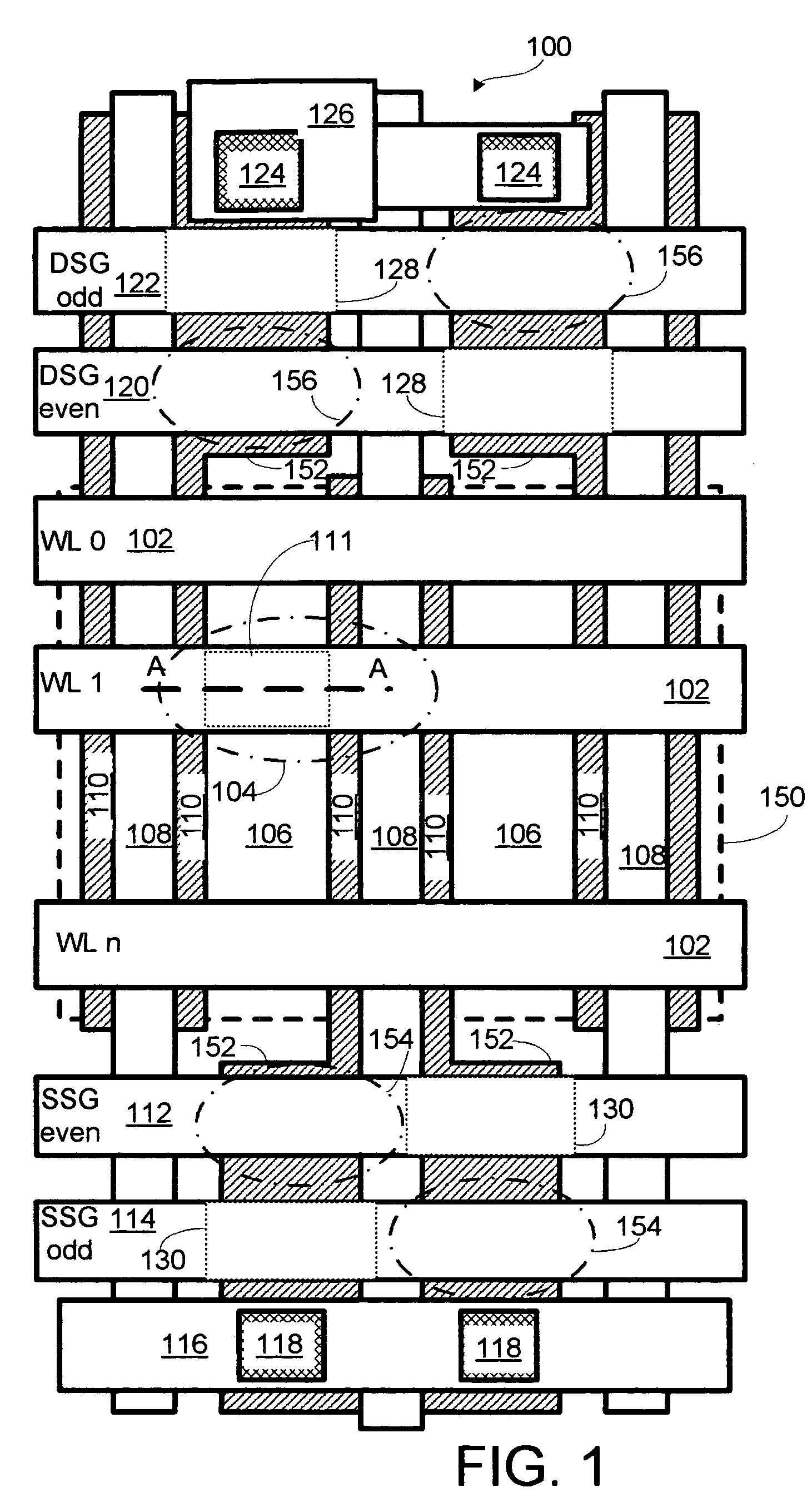
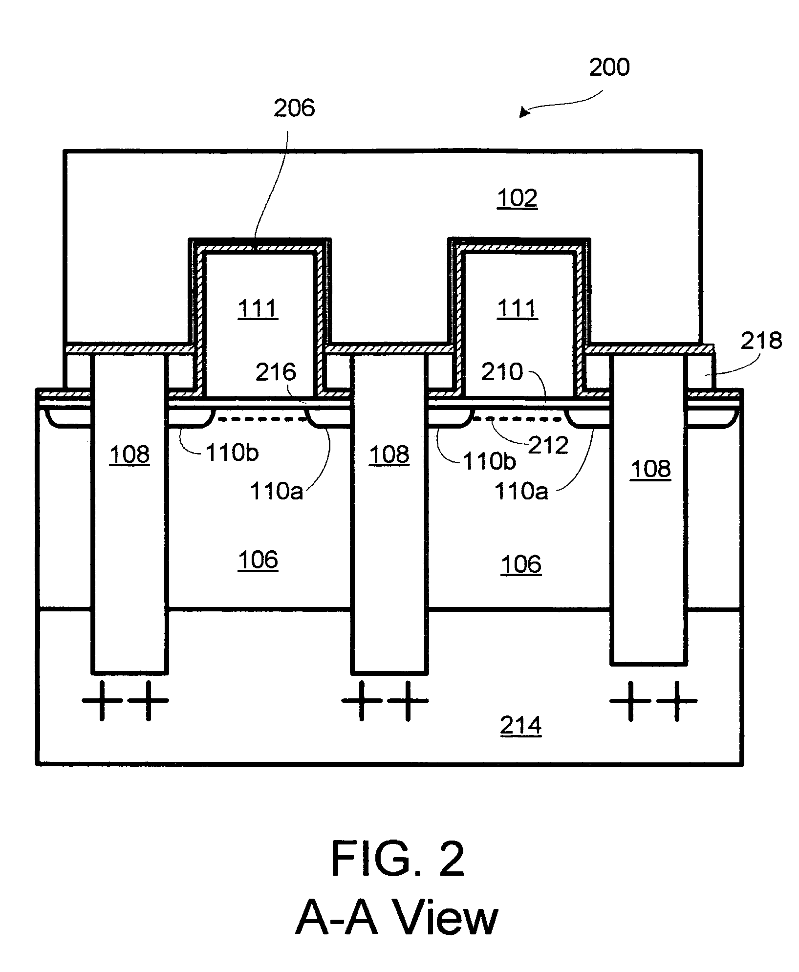
[0019]FIG. 1 illustrates a Flash EEPROM array 100. The Flash EEPROM array 100 includes a plurality of word select lines 102 running horizontally, a plurality of well regions 106 running vertically across several word lines, and a plurality of diffusion regions 110 running vertically along the well regions 106. Each well region 106 is surrounded by two deep trench isolation regions 108. Two diffusion regions 110 are placed on the top of each well region 106. One diffusion region 110 serves as a source and other diffusion region 110 serves as a drain. A floating gate 111 is placed between the diffusion regions 110 and under the word select line 102. The floating gate, the word select line 102, the well region 106, and two adjacent diffusion regions 110 form a memory cell 104. The Flash EEPROM array 100 also includes a plurality of source select gates 112, 114, and a plurality of data select gates 120, 122. A diffusion region 110 is connected to an extended diffusion region 152, which ...


PUM


Abstract

A multi-function memory array that includes a DRAM distributed in several DRAM sectors, a Flash EEPROM distributed in several Flash EEPROM sectors, a data bus interconnecting the DRAM sectors and the Flash EEPROM sectors, and a plurality of memory access control circuitries. Each DRAM sector and Flash EEPROM sector can be accessed independently and data can be transferred between a DRAM sector and a Flash EEPROM sector. External data can also be written into either DRAM or Flash EEPROM. Flash EEPROM in one sector is distributed in rows and columns, and cells in each column are separated from the cells in an adjacent column by deep trench isolation regions.

Description

BACKGROUND OF THE INVENTION[0001]1. Field of the Invention[0002]The present invention relates to logic gate structures, and particularly, to a Flash electrically erasable and programmable read-only memory (Flash EEPROM) and its use in a multi-function memory array.[0003]2. Description of the Related Art[0004]Electrically erasable and programmable non-volatile semiconductor devices, such Flash EEPROMs are well known in the art. One type of Flash EEPROM employs metal-oxide-semiconductor (MOS) floating gate devices. Typically, an electrical charge is transferred into an electrically isolated (floating) gate to represent one binary state, while an uncharged gate represents the other binary state. The floating gate is generally placed above and between two regions (source and drain) spaced-apart from each other and separated from those regions by a thin insulating layer, such as a thin oxide layer. An overlying gate is disposed above the floating gate provides capacitive coupling to the ...

Claims


Application Information

Patent Timeline
Patent Type & Authority Patents(United States)
IPC IPC(8): H01L23/62H01L29/93
CPCH01L27/115H01L27/11521H01L27/11524H01L29/66825H01L29/7881H10B69/00H10B41/35H10B41/30
Inventor YU, ANDYGO, YING W.
Owner SOOCHOW CAPITAL
Why Eureka
Try Eureka