

Electropolymerization of enhanced electrochromic (EC) polymer film
a technology of enhanced electrochromic and polymer film, applied in the field of electrochromic (ec) materials, can solve the problem that the opaque counter-electrode is not desirable for use in many ec devices, and achieve the effect of high lateral resolution
- Summary
- Abstract
- Description
- Claims
- Application Information
AI Technical Summary
Benefits of technology
Problems solved by technology
Method used
Image

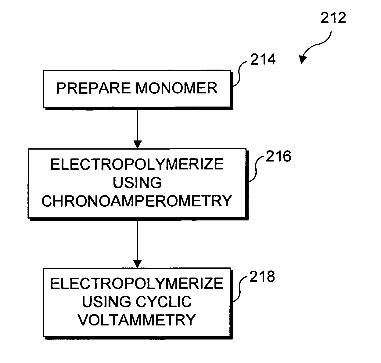
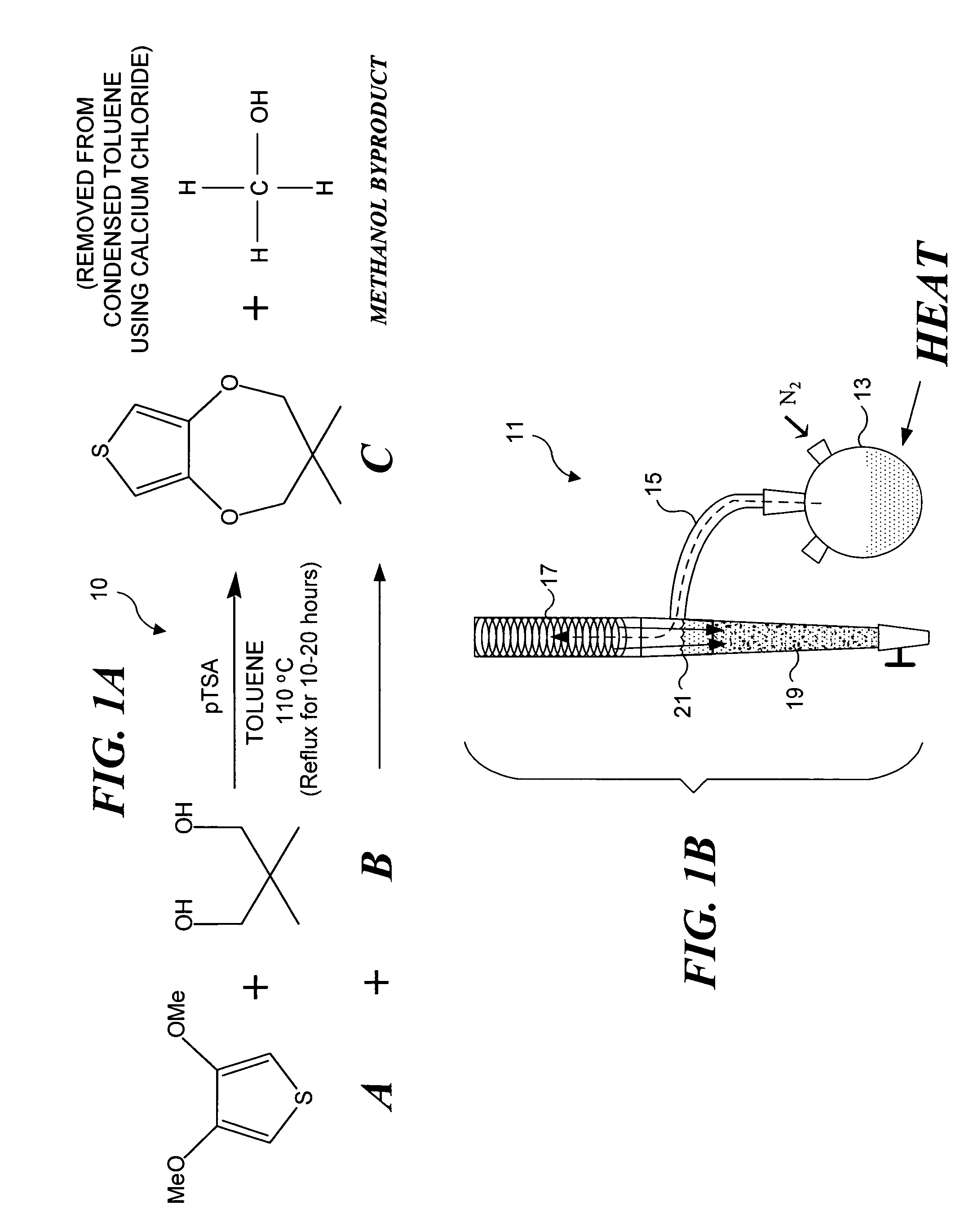
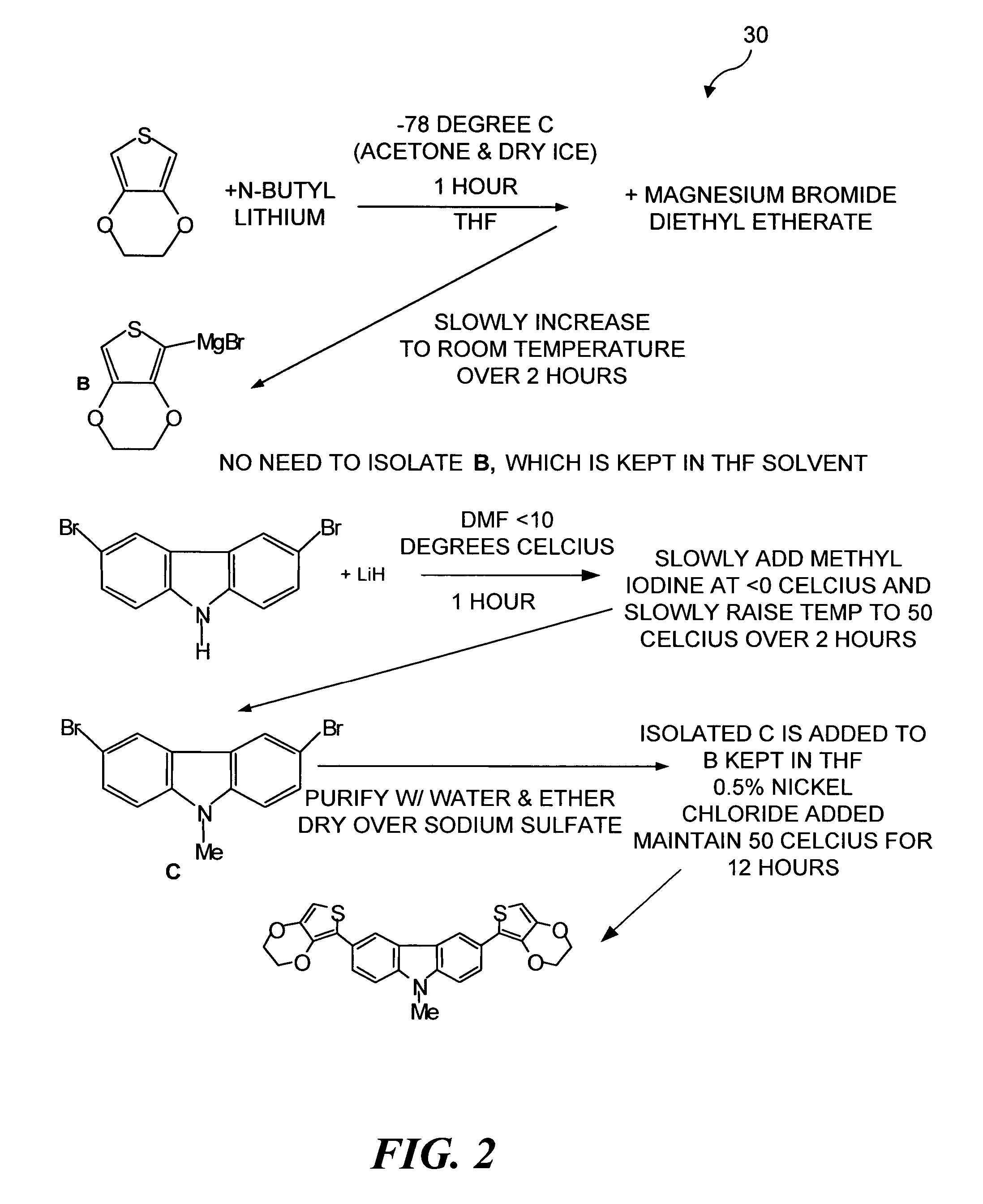
Examples
first embodiment
[0106]As noted above, highly conductive carbon (such as graphite) based counter-electrodes can also be employed. a highly conductive carbon based counter-electrode is shown in FIGS. 6C and 6D. Once again, a preferred substrate is a polished float glass cuvette plate, about 0.7 mm thick. An ITO coating 64 is applied on one side of the polished float glass cuvette plate, and a carbon coating 62 is then applied over the ITO coating. Preferably, the highly conductive carbon material is graphite (HITASOL GA.66M). The electrical conductivity of this highly conductive carbon material is known to be not less than 10−2 S / cm. Preferably, less than 25 percent of the glass substrate is covered with the carbon, in order to maintain high transmittance. While lithography and sputtering were employed for gold patterning on glass substrate as described above, screen printing was employed for forming a graphite pattern on a glass substrate for the highly conductive carbon-based counter-electrode. It ...
second embodiment
[0112]A sample device based on the single polymer / counter-electrode EC device described above was constructed using rectangular layers substantially 7 mm×50 mm. An ITO coated 7 m×50 mm glass slide was prepared for the transparent electrode, and a layer of PProDOT-Me2 was deposited on the ITO coated surface. A glass wafer onto which a grid pattern of gold had been deposited was cut into 7 mm×50 mm plates. Similar 7 mm×50 mm plates of graphite deposited in a grid pattern were also prepared. A PMMA / LiClO4 gel electrolyte was uniformly placed between the cathodic EC polymer deposited on the ITO slide and the counter-electrode to form a layered device. Two devices were prepared, one with a gold counter-electrode, and one with a graphite counter-electrode layer. The graphite based counter-electrode differs from the gold based counter-electrode in that a layer of ITO was first placed on the glass substrate before the graphite was deposited, while no such layer was employed in the gold base...
PUM
| Property | Measurement | Unit |
|---|---|---|
| voltage | aaaaa | aaaaa |
| thickness | aaaaa | aaaaa |
| temperature | aaaaa | aaaaa |
Abstract
Description
Claims
Application Information