Optical calibration system and method

a technology of optical calibration and optical device, applied in the field of optical calibration system and method, can solve the problems of increasing the bandwidth of fiber optic communication network, limiting the functionality of dwdm applications, and increasing the demand for network functionality, so as to reduce the effect of cross-talk

Active Publication Date: 2008-11-25
II VI DELAWARE INC
View PDF5 Cites 49 Cited by
  • Summary
  • Abstract
  • Description
  • Claims
  • Application Information

AI Technical Summary

Benefits of technology

[0041]In accordance with a third aspect of the invention, there is provided an optical system including: an optical input port for projecting an input optical signal onto an optical phased matrix array, an optical phased matrix array including a plurality of individually addressable pixels thereon, each pixel being drivable within a prescribed range of levels, and a plurality of optical output ports, each for collecting a predetermined fraction of the optical signal received from the optical phased matrix array; there is provided a method of minimizing variations in the fractional signal collected by the output ports including the steps of:
[0047]In accordance with a third aspect of the invention, there is provided an optical system including: an optical input port for projecting an input optical signal onto an optical phased matrix array, an optical phased matrix array including a plurality of individually addressable pixels thereon, each pixel being drivable within a prescribed range of levels, an optical output port for collecting a predetermined fraction of the optical signal received from the optical phased matrix array, a plurality of pixel transfer functions relating the level of each pixel to the phase variation each pixel introduces to light from the input optical signal which is incident thereon, and at least one routing transfer function describing the phase variation to be imparted by selected ones of the pixels to thereby couple the fraction of the optical signal between the input port and the output port, where the routing transfer function is constrained between selected minimum and maximum levels; there is provided a method of minimizing time-varying variations including the steps of:
[0049](b) modifying the maximum and minimum levels to substantially minimize the time-varying variations.
[0076](c3) determining a second modification function to modify the transfer functions of step (c1) to substantially minimize the effect of cross-talk on adjacent ones of the output ports.

Problems solved by technology

The increased bandwidth of fiber optic communication networks is still often insufficient to cope with this demand without utilizing the ability of these fibers to carry large numbers of individual communication channels, each identified by a discrete wavelength and each channel with a known bandwidth and separation from its adjacent channels.
The disadvantage associated with DWDM networks is that the increasing density of wavelength channels places increasing demand on network functionality for connecting the individual channels to individual destination points on a dynamic basis, and for the ability to add or drop an individual wavelength channel into or out of the optical signal.
Standard liquid crystal devices are limited in the pixel density and fill factors that can be efficiently manufactured, thus severely limiting their functionality in DWDM applications.
However, these devices are then limited to use in switching signals containing a predetermined number of channels i.e. a MEMS device that has been constructed for use in a system containing 64 individual wavelength channels cannot then be readily used where the signal contains 128 wavelength channels.
A difficulty in transplanting this technology arises when the operating environments of LCoS devices in display applications is compared with that of telecommunications applications.
Problems that can occur in the application of liquid crystal devices to DWDM switching applications can be attributed not only to irregularities in the liquid crystal device itself such as irregular phase response between pixels, but rather to aberrations from the surrounding optical elements as well.
For example, surface irregularities of the optical elements or slight misalignments of the optical system are common causes of wavefront aberration.
Edge effects in the SLM pixels can also adversely affect the device performance.
Another of the challenges that needs to be overcome with liquid crystal technology is the temperature stability over a broad range of operating conditions.

Method used


Image

  • Optical calibration system and method
  • Optical calibration system and method
  • Optical calibration system and method

Examples


Embodiment Construction

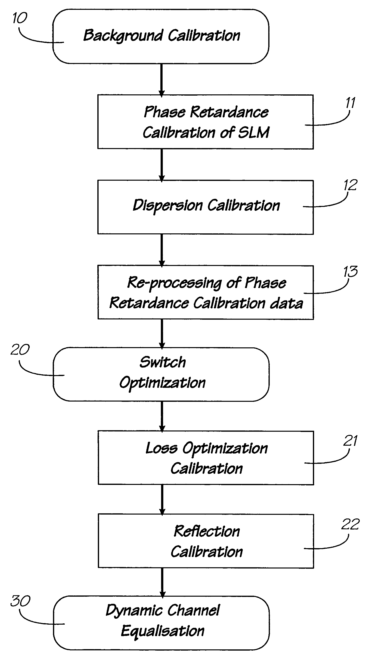
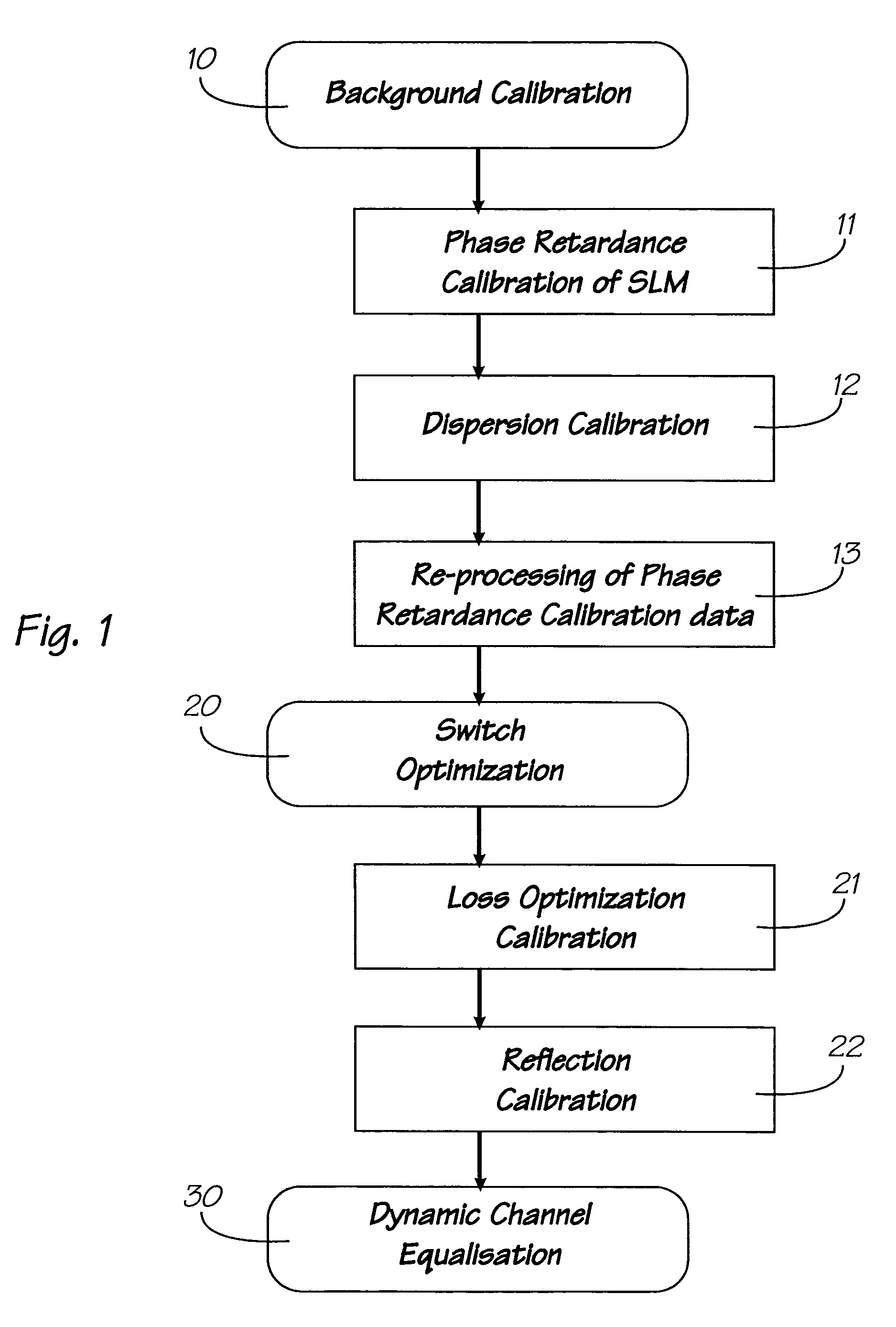
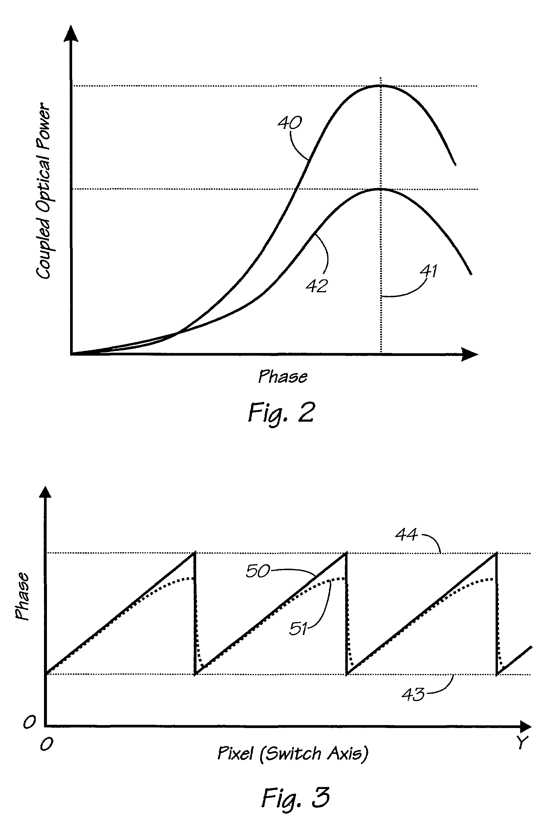
[0109]The preferred embodiment of the current device is a reconfigurable optical wavelength processor for use in telecommunications network applications. The optical processor uses a liquid crystal SLM (preferably a LCoS SLM) as an optical phased-matrix coupling device to couple selected wavelength channels contained in at least one optical input signal to at least one output port. The input and output ports, and the particular wavelength channels coupled between them, are chosen as required for the routing of signals in the telecommunications network. To ensure that the device is adaptable over a range of possible network configurations, the SLM is implemented as a dynamically reconfigurable grid. The individual pixels in the grid each modify the phase (or wavefront) of an incoming input beam in such a way that the beam is directed efficiently to a desired output port.

[0110]A self-calibration technique is described where the calibration of the optical processor is performed after t...


PUM


Abstract

In an optical system including an optical input port for projecting an input optical signal onto an optical phased matrix array, an optical phased matrix array including a plurality of individually addressable pixels thereon, each said pixel being drivable within a prescribed range of levels, and an optical output port for collecting a predetermined fraction of said optical signal received from said optical phased matrix array; a method of compensating for phase distortions including the steps of: (a) determining a plurality of transfer functions relating said level of each said pixel to the phase variation each said pixel introduces to light from said input optical signal which is incident thereon; and (b) controlling the level of selected ones of said pixels in accordance with a corresponding transfer function such that said fractional signal received at said output port is modified in phase to substantially compensate for optical phase distortions arising from said optical phased matrix array.

Description

CO-PENDING APPLICATIONS[0001]Various methods, systems and apparatus relating to the present invention are disclosed in the following co-pending applications filed by the applicant or assignee of the present invention: U.S. application Ser. No. 10 / 706901 filed on 12 Nov. 2003; U.S. application Ser. No. 10 / 868521 filed on 14 Jun. 2004; U.S. application filed on 27 Sep. 2004 under Ser. No. 11 / 952,223; and Australian application 2004904650 filed on 16 Aug. 2004. The disclosures of these co-pending applications are incorporated herein by cross-reference.FIELD OF THE INVENTION[0002]The current invention relates to calibration methods for optical devices, and in particular to calibration methods for reconfigurable optical wavelength processing devices for use in telecommunications applications which incorporate a liquid crystal spatial light modulator (SLM).BACKGROUND OF THE INVENTION[0003]The recent growth in the demand for broadband services has resulted in a pressing need for increased ...

Claims


Application Information

Patent Timeline
Patent Type & Authority Patents(United States)
IPC IPC(8): H04B10/00
CPCG01M11/0292G02B6/29311G02B6/29313G02F2203/50G02F2203/12
Inventor FRISKEN, STEVEN J.BAXTER, GLENN W.ZHOU, HAOABAKOUMOV, DMITRI
Owner II VI DELAWARE INC
Why Eureka
Try Eureka