Stiffener for flip chip BGA package

a technology of flip chip and flip chip, which is applied in the direction of semiconductor devices, semiconductor/solid-state device details, electrical devices, etc., can solve the problems of package structure bowing, exacerbated problems, and subject to different temperatures, so as to improve the reliability of the package, less bowing, and improved co-planarity

Active Publication Date: 2008-12-02
ALTERA CORP
View PDF38 Cites 61 Cited by
  • Summary
  • Abstract
  • Description
  • Claims
  • Application Information

AI Technical Summary

Benefits of technology

[0007]To achieve the foregoing, the present invention provides semiconductor die flip chip packages with warpage control. The present invention also provides fabrication methods for such packages. In general, a package includes a stiffener that is made of a material that complements the other components in the package by managing the package stresses due to CTE mismatches between various package components. For example, the stiffener may have a material with a relatively low CTE value and / or mass density value as compared to conventional stiffener materials such as copper. The result is a package with less bowing and so improved co-planarity (e.g., in compliance with industry specifications) with the surface to which it is ultimately bound; thereby, improving the reliability of the package. Moreover, a package that is relatively lighter and more robust than conventional semiconductor die flip chip packages can be realized.

Problems solved by technology

A problem with such a semiconductor die flip chip package is that it is subject to different temperatures during the packaging process.
The high stress experienced by bonded materials during cooling may cause them to warp or crack and cause the package structure to bow.
In addition, this problem is exacerbated in the case of a relatively thick die processed from a larger diameter wafer, for example a 300 mm diameter wafer.
However, the thinner package substrates are more susceptible to the stress resulting from CTE mismatches of materials within the package.
Further, with the advent of low-K dice, the high stress caused by the different CTE is even more of a concern.
Low-K dielectric material layers in the low-K die are relatively brittle, rendering the low-K die susceptible to failure at even lower stress levels than conventional dice with FSG or USG dielectrics.

Method used


Image

  • Stiffener for flip chip BGA package
  • Stiffener for flip chip BGA package

Examples


example

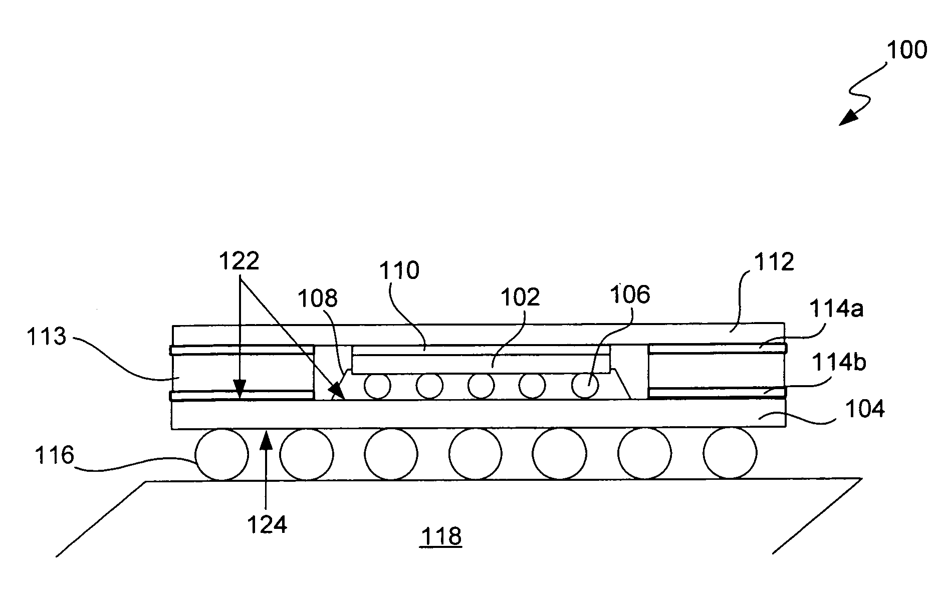
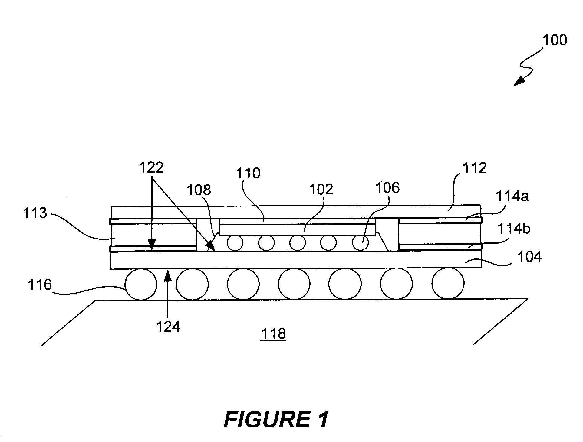
[0038]The following example provides modeling results for a semiconductor die flip chip package with warpage control in accordance with specific embodiments of the present invention. It should be understood the following is representative only, and that the invention is not limited by the detail set forth in this example.

[0039]A Stratix II device, available from Altera, Inc. of San Jose, Calif., was selected in modeling a semiconductor die flip chip package in accordance to the present invention. The Stratix II device included a 40 mm×40 mm FCBGA package with a die (22 mm×22 mm; 0.78 mm thick) and a package substrate (3-2-3 buildup type; 0.8 mm thick core). It should be noted that the package substrate is also available from Kyocera of Kyoto, Japan. The die had a CTE of about 2.6-3 ppm / ° C. whereas the package substrate had a CTE of about 17-18 ppm / ° C. Other significant CTE values included: underfill (32 ppm / ° C.); heat spreader (17 ppm / ° C.). The heat spreader was 0.5 mm thick whe...


PUM


Abstract

Provided are semiconductor die flip chip packages with warpage control and fabrication methods for such packages. A package includes a heat spreader that is attached to a die and a stiffener, which are in turn attached to a package substrate. In general, the stiffener is made of a material that has a relatively low CTE value. For example, the stiffener material may have a CTE value less than 12 ppm / ° C. The material may also have a relatively low mass density value of less than 8.9 g / cm3. Such a material may include natural graphite or some composite form of it. The result is a package with less bowing and so improved co-planarity (e.g., in compliance with industry specifications) with the surface to which it is ultimately bound; thereby, improving the reliability of the package. Moreover, a package that is relatively lighter and more robust than conventional semiconductor die flip chip packages can be realized.

Description

BACKGROUND[0001]This invention relates generally to semiconductor device package assembly, and in particular to semiconductor die flip chip package assembly. More specifically, the invention relates to an innovative material approach for a stiffener to reduce weight and warpage in a flip chip ball grid array (BGA) package.[0002]In semiconductor device package assembly, a semiconductor die (also referred to as an integrated circuit (IC) chip or “chip”) may be bonded directly to a package substrate. Such die is formed with bumps of solder affixed to its I / O bonding pads. During packaging, the die is “flipped” onto its front surface (e.g., active circuit surface) so that the solder bumps form electrical and mechanical connections directly between the die and conductive metal pads on the package substrate. Underfill is generally applied between the gap formed by the solder bumps in order to further secure the die to the package substrate. A stiffener made of substantially copper is then...

Claims


Application Information

Patent Timeline
Patent Type & Authority Patents(United States)
IPC IPC(8): H01L23/14
CPCH01L23/36H01L23/373H01L23/49833H01L23/3128H01L2224/16H01L2224/73253H01L2924/15311H01L2924/16195H01L2924/01019H01L2924/01322H01L2224/73204H01L2224/16225H01L2224/32225H01L2924/00H01L2224/32245H01L2924/10253H01L2924/00011H01L2924/00014H01L2224/0401
Inventor LI, YUAN
Owner ALTERA CORP
Why Eureka
Try Eureka