Nonvolatile semiconductor memory device and programming or erasing method therefor

a nonvolatile semiconductor and memory device technology, applied in static storage, digital storage, instruments, etc., can solve the problems of lowering the access speed, erroneous data read in the market, and deteriorating retention characteristics, so as to improve the subsequent data retention characteristic and the effect of data retention characteristi

Active Publication Date: 2008-12-02
PANASONIC SEMICON SOLUTIONS CO LTD
View PDF11 Cites 71 Cited by
  • Summary
  • Abstract
  • Description
  • Claims
  • Application Information

AI Technical Summary

Benefits of technology

[0017]An object of the present invention is suppressing deterioration of the data retention characteristic of nonvolatile semiconductor memory cells having a trap layer.
[0019]According to the present invention, in a programming or erasing sequence, first charge injection with a given wait time being secured and second charge injection following the first charge injection are executed. With this sequence, surrounding charge that may deteriorate the data retention characteristic is reduced by use of initial variation occurring immediately after the charge injection operation (charge loss phenomenon due to binding of the injected charge with the surrounding charge in an extremely short time), and then the charge loss due to the initial variation is compensated, to thereby improve the subsequent data retention characteristic.

Problems solved by technology

The data retention characteristic deteriorates with this change in memory cell threshold voltage, and this causes lowering of the access speed and erroneous read of data in the market.

Method used


Image

  • Nonvolatile semiconductor memory device and programming or erasing method therefor
  • Nonvolatile semiconductor memory device and programming or erasing method therefor
  • Nonvolatile semiconductor memory device and programming or erasing method therefor

Examples


embodiment 2

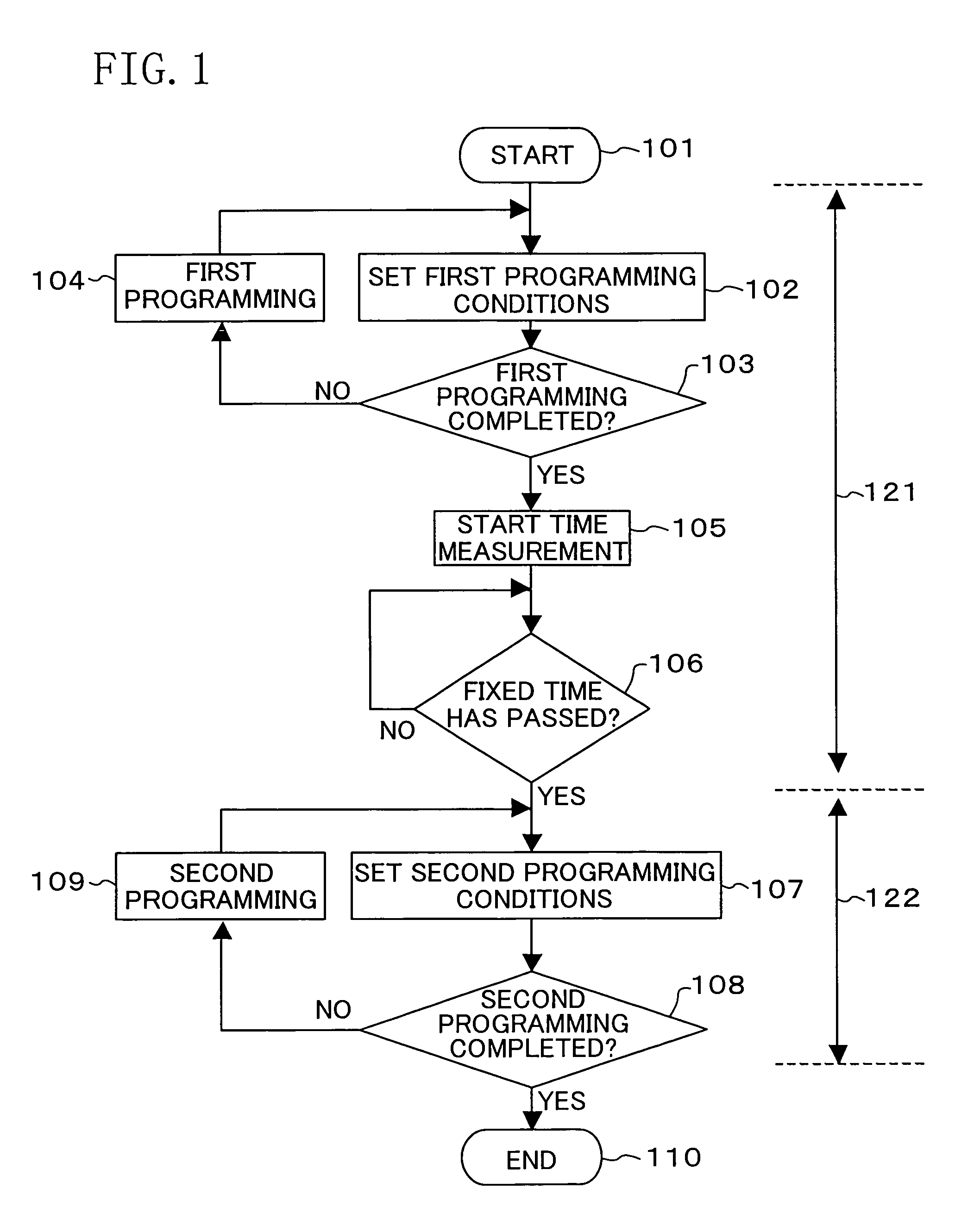
[0074]FIG. 6 is a flowchart showing a programming or erasing method for a nonvolatile semiconductor memory device in Embodiment 2 of the present invention. Hereinafter, a method adopted when programming is made for a particular nonvolatile memory cell will be described.

[0075]In the flowchart of FIG. 6, a block 611 is for deciding whether or not the first charge injection has been executed a predetermined number of times.

[0076]Once completion of the first programming is decided in the decision 103, the processing 105 of starting time measurement is executed. Whether or not a fixed time has passed from the start of time measurement is determined in the decision 106. If the fixed time has passed, then the flow proceeds to the decision 611 of determining whether or not the first charge injection has been executed a predetermined number of times. If it is determined in the decision 611 that the first charge injection has been executed a predetermined number of times, the flow proceeds to...

embodiment 3

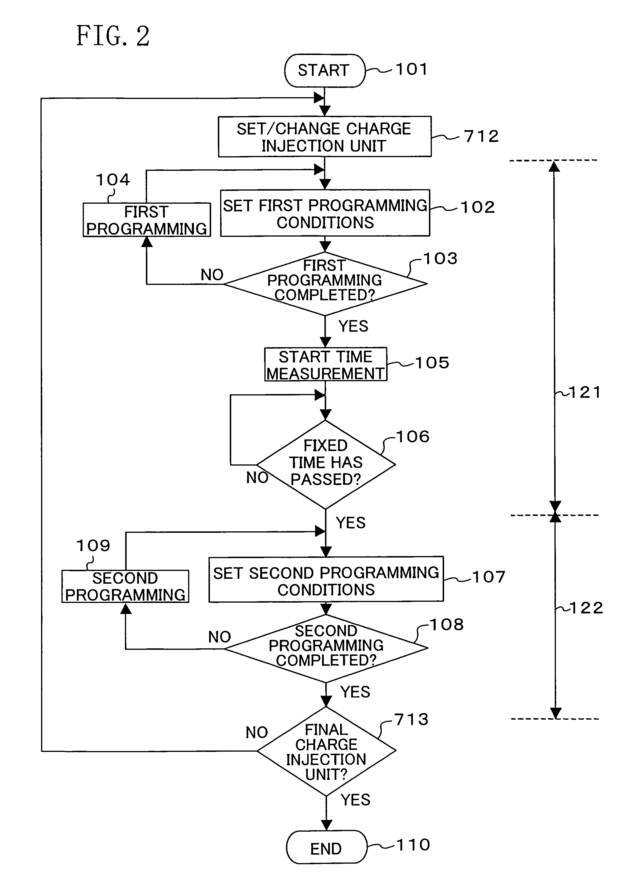
[0083]FIG. 8A shows an execution sequence in Embodiment 3 of the present invention. Referring to FIG. 8A, a fixed time 923 is secured from completion of first programming 921 until start of second programming 922. Note that the first charge injection corresponds to a range 911 including the first programming 921 and the fixed time 923 and the second charge injection corresponds to a range 912 including the second programming 922. A longer fixed time 923 is more desirable. In particular, the fixed time 923 may be a time longer than the time required for normal verify operation or read operation, or a time in which electrons trapped under the first programming have been bound with surrounding charge (holes) already trapped before the first programming.

[0084]In programming for a memory cell array, however, if the sequence of FIG. 8A is executed serially for a plurality of addresses, the time required for programming will disadvantageously increase. In Embodiment 3, this problem can be ...

embodiment 4

[0099]In Embodiment 4, both the first programming and the second programming are executed under given conditions without verify operation. In such programming under given conditions, programming is performed with the programming or erasing voltage and the pulse width being fixed, for example.

[0100]FIGS. 10A through 10H show a programming or erasing method for a nonvolatile semiconductor memory device in Embodiment 4 of the present invention. Hereinafter, a method adopted when programming is made for a particular nonvolatile memory cell will be described.

[0101]FIGS. 10A through 10D show distributions of the memory cell threshold voltage, where the x-axis represents the memory cell threshold voltage and the y-axis represents the number of memory cells targeted for programming. FIGS. 10E through 10H show the probability density distributions in the neighborhood of the first impurity region 1803 in FIG. 19, where the x-axis represents the distance in the direction of arrow x in FIG. 19 ...


PUM


Abstract

In a nonvolatile memory cell having a trap layer, programming or erasing is made in a sequence of first charge injection with a given wait time being secured and second charge injection executed after the first charge injection. Surrounding charge that deteriorates the data retention characteristic is reduced by use of initial variation occurring immediately after programming (charge loss phenomenon due to binding of injected charge with the surrounding charge in an extremely short time), and then the charge loss due to the initial variation is compensated, to thereby improve the data retention characteristic.

Description

BACKGROUND OF THE INVENTION[0001]The present invention relates to an electrically programmable, erasable nonvolatile semiconductor memory device having a trap layer in a gate insulation film formed between a channel region and a gate electrode of each memory cell transistor, and a programming or erasing method for such a semiconductor memory device.[0002]In a conventional nonvolatile memory having a trap layer, electric charge (electrons and holes) is trapped by injection of the charge in a discrete trap layer (a SiN film or a transition region at the interface of a SiN film / a top SiO2 film) existing inside an insulating film (SiO2) formed between a channel region and a gate electrode of a memory cell. Data “0” or data “1” is determined with respect to the threshold voltage of the memory cell, to thereby store information.[0003]Hereinafter, description will be made regarding injection of electrons as programming (write) while injection of holes as erasing, and also regarding injecte...

Claims


Application Information

Patent Timeline
Patent Type & Authority Patents(United States)
IPC IPC(8): G11C16/00
CPCG11C16/349
Inventor NAGAI, HIROYASUTOKI, MASAHIROMISUMI, KENJIKOTANI, HIDETO
Owner PANASONIC SEMICON SOLUTIONS CO LTD
Why Eureka
Try Eureka