Nitride semiconductor light emitting device

a light-emitting device and semiconductor technology, applied in the direction of semiconductor devices, basic electric elements, electrical appliances, etc., can solve the problems of deteriorating the luminance of the light-emitting device, crystal defects, siosub>2 /sub>, etc., and achieve the effect of low density and high quality

Active Publication Date: 2008-12-09
SAMSUNG ELECTRONICS CO LTD
View PDF3 Cites 13 Cited by
  • Summary
  • Abstract
  • Description
  • Claims
  • Application Information

AI Technical Summary

Benefits of technology

[0009]The present invention has been made in view of the above problems, and it is an object of the present invention to provide a high quality nitride semiconductor light emitting device, which has a low density of crystal defects in a nitride semiconductor crystal, particularly, in an active layer.
[0010]It is another object of the present invention to provide the nitride semiconductor light emitting device which exhibits high luminance and excellent reliability.
[0016]According to yet another embodiment of the present invention, the intermediate layer may have the multilayer structure in which laminates of AlGaN / GaN / InGaN / GaN layers are repetitiously stacked, the AlGaN / GaN / InGaN / GaN layers constituting one stacking cycle in the multilayer structure. The GaN layer interposed between the AlGaN layer and the InGaN layer serves to relieve stress from the AlGaN and InGaN layers, thereby more effectively prevent formation of the crystal defects.

Problems solved by technology

However, the nitride semiconductor such as the GaN semiconductor is generally grown on a heterogeneous substrate such as a sapphire substrate, and thus suffers from crystal defects due to lattice mismatch between the semiconductor material and the heterogeneous substrate.
The crystal defects provide an adverse influence on reliability (for example, tolerance to electrostatic discharge ESD) of the light emitting device, and deteriorate the luminance of the light emitting device via absorption of light.
Although various attempts including a selective epitaxial growth method have been progressed to prevent the crystal defects, these attempts have problems of a complicated process such as deposition of SiO2 mask, and high manufacturing costs.
Even with the buffer layer 13, however, the problems caused by the crystal defects within the light emitting device 10 cannot be satisfactorily solved.
A significant density of crystal defects remains in the nitride semiconductor crystal, in particular, in the active layer.
The crystal defects not only obstruct light emission from the active layer through absorption of light, but also reduce a reverse breakdown voltage or a tolerance voltage to reverse ESD.
In this manner, the crystal defects deteriorate the luminance and reliability of the light emitting device.

Method used


Image

  • Nitride semiconductor light emitting device
  • Nitride semiconductor light emitting device
  • Nitride semiconductor light emitting device

Examples


embodiment 1

[0043]FIG. 4 is a partially cross-sectional view of a multilayered intermediate layer according to a first embodiment of the invention, and FIG. 5 is a graph depicting one example of a band-gap profile of the multilayered intermediate layer of FIG. 4.

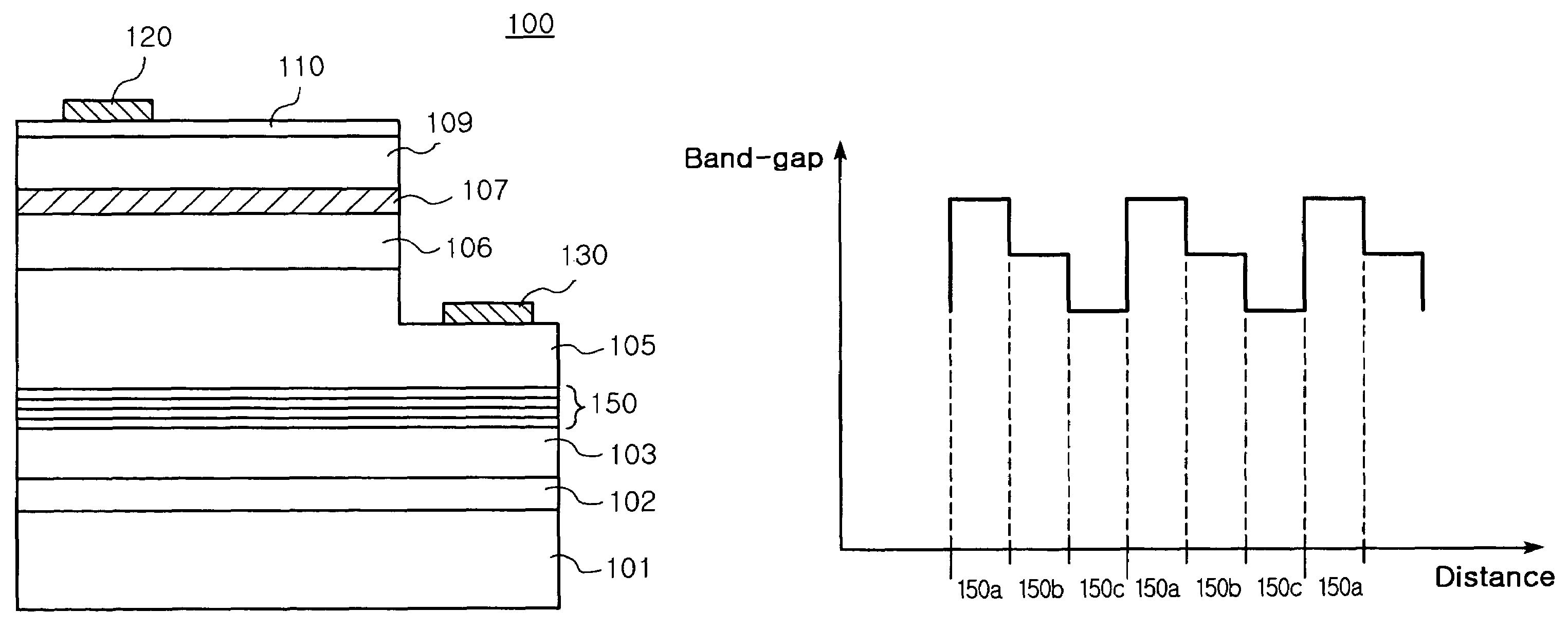
[0044]Referring to FIGS. 4 and 5, the multilayered intermediate layer 150 comprises a laminate of an AlGaN layer 150a, a GaN layer 150b and an InGaN layer 150c, which are sequentially stacked therein. In particular, laminates of the AlGaN layer 150a, GaN layer 150b and InGaN layer 150c are repetitiously stacked in the intermediate layer 150. In this embodiment, the AlGaN / GaN / InGaN layers 150a, 150b and 150c constitute one stacking cycle in the multilayer structure. Preferably, the intermediate layer 150 has the super lattice structure. Among the nitride semiconductor layers 150a, 150b and 150c constituting the intermediate layer 150, the AlGaN layer 150a has the highest band-gap, and the InGaN layer 150c has the lowest band-gap. The GaN...

embodiment 2

[0048]FIG. 6 is a partially cross-sectional view of a multilayered intermediate layer according to a second embodiment of the invention, and FIG. 7 is a graph depicting one example of a band-gap profile of the multilayered intermediate layer of FIG. 6. In terms of sequence of stacking layers for the intermediate layer, the intermediate layer of the second embodiment is different from that of the first embodiment.

[0049]Referring to FIGS. 6 and 7, laminates of an InGaN layer 150c, a GaN layer 150b and an AlGaN layer 150a are repetitiously stacked on a first nitride semiconductor layer 103. In this embodiment, the InGaN / GaN / AlGaN layers 150c, 150b and 150a constitute one stacking cycle in the multilayer structure. Preferably, the intermediate layer 150 has the super lattice structure. As shown in FIG. 7, the nitride semiconductor layers of the intermediate layer 150 are repetitiously stacked in the sequence of InGaN / GaN / AlGaN layers 150c, 150b and 150a (opposite to that of the first em...

embodiment 3

[0052]FIG. 8 is a partially cross-sectional view of a multilayered intermediate layer according to a third embodiment of the invention, and FIG. 9 is a graph depicting one example of a band-gap profile of the multilayered intermediate layer of FIG. 8. According to the third embodiment, the intermediate layer comprises a GaN layer interposed between an AlGaN layer and an InGaN layer so as not to form an AlGaN / InGaN interface.

[0053]Referring to FIGS. 8 and 9, laminates of AlGaN / GaN / InGaN / GaN layers 150a, 150b, 150c and 150b are repetitiously stacked on a first nitride semiconductor layer 103. In this embodiment, the AlGaN / GaN / InGaN / GaN layers 150a, 150b, 150c and 150b constitute one stacking cycle in the multilayer structure. Preferably, the intermediate layer 150 has the super lattice structure. As shown in FIG. 9, the GaN layer 150b is interposed between the AlGaN layer 150a of a higher band-gap and the InGaN layer 150c of a lower band-gap so as not to form the AlGaN / InGaN interface...


PUM


Abstract

Disclosed herein is a nitride semiconductor light emitting device, which is improved in luminance and reliability. The light emitting device, comprises an n-type nitride semiconductor layer, an active layer and a p-type nitride semiconductor layer sequentially formed on a substrate, an n-side electrode formed on a portion of an upper surface of the n-type nitride semiconductor layer, and at least one intermediate layer formed between the substrate and the n-type nitride semiconductor layer. The intermediate layer has a multilayer structure of three or more layers having different band-gaps, and is positioned below the n-side electrode.

Description

RELATED APPLICATION[0001]The present invention is based on, and claims priority from, Korean Application Number 2005-132248, filed on Dec. 28, 2005, the disclosure of which is incorporated by reference herein in its entirety.BACKGROUND OF THE INVENTION[0002]1. Field of the Invention[0003]The present invention generally relates to a nitride semiconductor light emitting device, and, more particularly, to a nitride semiconductor light emitting device, which is reduced in crystal defects, and has improved luminance and reliability.[0004]2. Description of the Related Art[0005]Recently, a group III-V nitride semiconductor, such as a GaN semiconductor, has been in the spotlight as an essential material for light emitting devices, such as light emitting diodes (LEDs), laser diodes (LDs), and the like, due to its excellent physical and chemical properties. The III-V nitride semiconductor material comprises a GaN-based material having the formula InxAlyGa(1-x-y)N (where 0≦x≦1, 0≦y≦1, 0≦x+y≦1)...

Claims


Application Information

Patent Timeline
Patent Type & Authority Patents(United States)
IPC IPC(8): H01L33/00H01L33/06H01L33/12H01L33/14H01L33/32
CPCH01L33/04H01L33/32
Inventor HAN, SANG HEONOH, BANG WONKIM, JE WONSHIM, HYUN WOOKKANG, JOONG SEOLEE, DONG JU
Owner SAMSUNG ELECTRONICS CO LTD
Why Eureka
Try Eureka