Manufacturing method of GaN substrate laser diode

A laser diode and substrate technology, applied in the structural details of semiconductor lasers, etc., can solve problems such as crystal strain, shortened laser diode life, and reduced quality and performance of the epitaxial layer on the substrate

Inactive Publication Date: 2013-01-02
JIANGSU WINAD LIGHTING TECH
View PDF1 Cites 1 Cited by
  • Summary
  • Abstract
  • Description
  • Claims
  • Application Information

AI Technical Summary

Problems solved by technology

The above-mentioned semiconductor materials used as substrates generally contain various defects, such as dislocations, gaps or vacancies, etc. The defects will cau

Method used


Image

  • Manufacturing method of GaN substrate laser diode

Examples


Embodiment Construction

[0016] The present invention will be described in detail below in conjunction with the accompanying drawings and specific embodiments, but not as a limitation of the present invention.

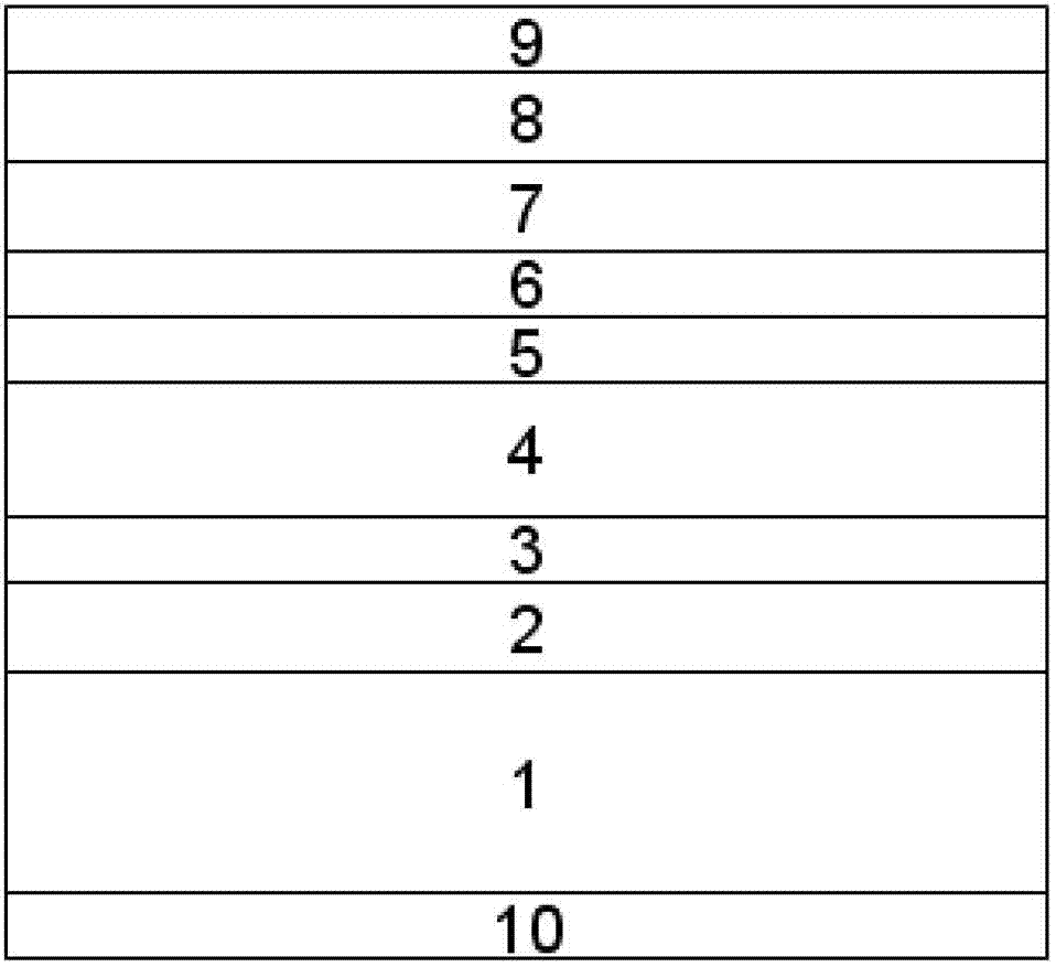
[0017] figure 1 A schematic diagram of the structure of the laser diode of the present invention is shown. It includes an n-GaN substrate 1 on which an n-type cladding layer 2 , an n-type light guide layer 3 and an active layer 4 are sequentially deposited.

[0018] The n-type cladding layer 2 is n-Al a In b Ga 1-a-b N, the optical guiding layer 3 is n-Al c In d Ga 1-c-d N, where 0≤a, b, c, d, a+b, c+d≤1.

[0019] The cladding layer 2 can also be n-Al a In b Ga 1-a-b N superlattice.

[0020] Active layer 4 is n-Al with superlattice structure e In f Ga 1-e-f N / n-AI g In h Ga 1-g-h N multiple quantum well layers, where 0≤e, f, g, h, e+f, g+h≤1.

[0021] A p-type barrier layer 5 is also deposited on the active layer 4, and the p-type barrier layer 5 is

[0022] p-Al i In j Ga...


PUM


Abstract

The invention discloses a manufacturing method of a GaN substrate laser diode. The manufacturing method comprises the following steps of: forming a GaN substrate, and sequentially depositing an n type coating layer, an n type light guide layer, an active layer, a p type barrier layer, a p type light guide layer and a p type coating layer, wherein the method for forming the GaN substrate comprises the steps of putting a GaN wafer into a high-temperature and high-pressure device, and pressurizing the GaN wafer when heating the GaN wafer, wherein the heating temperature is 820-880 DEG C, the pressurizing pressure is 4.1-4.6 GPa, and the pressurizing is kept for 10-15min; stopping heating and pressurizing to enable the GaN wafer to restore to constant temperature and constant pressure; and after annealing in the high-temperature and high-pressure device for 20-30min, taking out the GaN wafer. With the adoption of the method, the crystal defect density in the laser diode substrate can be obviously reduced, the performance of the laser diode is improved, and the service life of the laser diode is prolonged.

Description

technical field [0001] The invention relates to a manufacturing method of a laser diode. Background technique [0002] A laser diode (LD) is a diode formed of semiconductor materials, and its basic structure includes a substrate and a P / N cladding layer deposited on the substrate in sequence, an active layer and a P / N cladding layer, and an N Ohmic contacts on the P-type and P-type cladding layers. As the foundation of the building of LD, the substrate plays an important role. Sapphire is a commonly used LD substrate, but due to the lattice and thermal stress mismatch between it and the heterogeneous epitaxial layer on it, it will crack due to different expansion degrees after heating, resulting in device damage. Another type of LD substrate includes GaN, GaAs, InP and other semiconductor materials. The above-mentioned semiconductor materials used as substrates generally contain various defects, such as dislocations, gaps or vacancies, etc. The defects will cause crystal ...

Claims


Application Information

Patent Timeline
IPC IPC(8): H01S5/02
Inventor 虞浩辉周宇杭
Owner JIANGSU WINAD LIGHTING TECH
Why Eureka
Try Eureka