SINGLE-CRYSTAL 4H-SiC SUBSTRATE

a single crystal, 4hsic technology, applied in single crystal growth, thin material processing, chemistry apparatus and processes, etc., can solve the problem of not knowing the method of reducing crystal defects, and achieve the effect of reducing the density of crystal defects

Active Publication Date: 2016-10-13
MITSUBISHI ELECTRIC CORP
View PDF3 Cites 1 Cited by
  • Summary
  • Abstract
  • Description
  • Claims
  • Application Information

AI Technical Summary

Benefits of technology

The present invention helps to reduce defects in high-quality silicon carbide substrates.

Problems solved by technology

Heretofore there has been no known method for reducing crystal defects in a single-crystal 4H-SiC substrate.

Method used


Image

  • SINGLE-CRYSTAL 4H-SiC SUBSTRATE
  • SINGLE-CRYSTAL 4H-SiC SUBSTRATE
  • SINGLE-CRYSTAL 4H-SiC SUBSTRATE

Examples


first embodiment

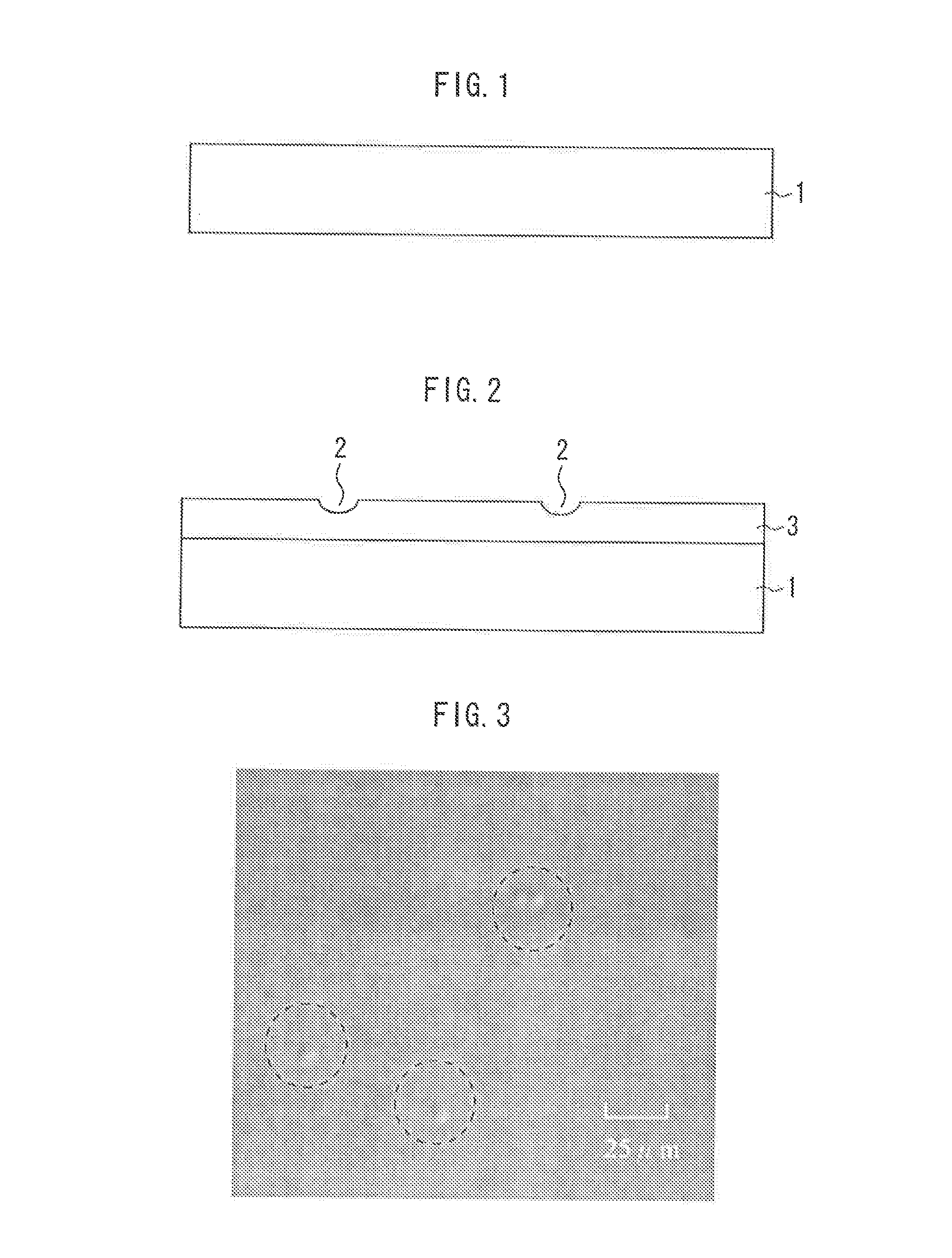
[0020]A method of manufacturing a single-crystal 4H-SiC substrate in accordance with a first embodiment of the present invention will be described. FIGS. 1 and 2 are cross-sectional views showing the method of manufacturing a single-crystal 4H-SiC substrate in accordance with the first embodiment.

[0021]The method begins by preparing a 4H-SiC bulk single-crystal substrate 1 misoriented by 4 degrees from the (0001) plane (or C-plane) toward a direction, as shown in FIG. 1. (The completed single-crystal 4H-SiC substrate of the present embodiment will have a principal surface in the (0001) plane.) It should be noted that the misorientation angle need not necessarily be 4 degrees, but may be in the range of 2-10 degrees.

[0022]Specifically, the 4H-SiC bulk single-crystal substrate 1 is planarized by mechanical polishing and chemical mechanical polishing using an acidic or alkaline solution. Further, the substrate 1 is ultrasonically cleaned using acetone to remove organic matter. The 4H-...

second embodiment

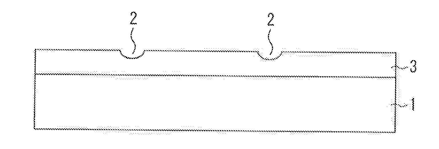
[0030]A method of manufacturing a single-crystal 4H-SiC substrate in accordance with a second embodiment of the present invention will be described. FIG. 7 is a cross-sectional view showing the method of manufacturing a single-crystal 4H-SiC substrate in accordance with the second embodiment.

[0031]First, as in the first embodiment, a single-crystal 4H-SiC layer 3 having a thickness of 300 nm is epitaxially grown so that that its growth surface has recesses 2. It should be noted that the thickness of the single-crystal 4H-SiC layer 3 need not necessarily be 300 nm, but may be in the range of from 50 nm to 10 μm. Then, as shown in FIG. 7, a single-crystal 4H-SiC layer 4 having a thickness of 10 μm is epitaxially grown on the single-crystal 4H-SiC layer 3 so as to bury the recesses 2.

[0032]Specifically, the single-crystal 4H-SiC layer 4 is formed by supplying SiH4 gas at a flow rate of 900 sccm and C3H8 gas at a flow rate of 360 sccm and further supplying nitrogen gas serving as an N-t...


PUM

PropertyMeasurementUnit
optimum growth temperatureaaaaaaaaaa
growth temperatureaaaaaaaaaa
misorientation angleaaaaaaaaaa

Abstract

A single-crystal 4H-SiC substrate includes a 4H-SiC bulk single-crystal substrate; and an epitaxial first single-crystal 4H-SiC layer on the 4H-SiC bulk single-crystal substrate and having recesses. The recesses have a diameter no smaller than 2 μm and no larger than 20 μm. The recesses have a depth no smaller than 0.01 μm and no larger than 0.1 μm. A single-crystal 4H-SiC substrate also includes a 4H-SiC bulk single-crystal substrate; and an epitaxial first single-crystal 4H-SiC layer on the 4H-SiC bulk single-crystal substrate and having recesses. The density of the recesses in the epitaxial first single-crystal 4H-SiC layer is at least 10 / cm2, and the epitaxial first single-crystal 4H-SiC layer has a defect density no larger than 2 / cm2.

Description

BACKGROUND OF THE INVENTION[0001]1. Field of the Invention[0002]The present invention relates to a single-crystal 4H-SiC substrate and method for manufacturing the same having a reduced crystal defect density.[0003]2. Background Art[0004]Recently, much attention has been given to the use of silicon carbide (or SiC) as a material primarily for power control devices, since SiC is superior to silicon in terms of breakdown field strength, saturated drift velocity, and thermal conductivity. Power devices formed of SiC can be configured to have substantially reduced power loss and a reduced size, allowing power saving in power conversion. Therefore, these power devices can be used to enhance the performance of electric vehicles and the functionality of solar cell systems, etc., and hence are a key element in creating a low-carbon society.[0005]The doping density and the thickness of a substrate on which an SiC power device is to be formed are determined substantially by the specifications...

Claims


Application Information

Patent Timeline
Patent Type & Authority Applications(United States)
IPC IPC(8): C30B29/36C30B29/68C30B25/20
CPCC30B29/36C30B29/68C30B25/20Y10T428/24612Y10T428/24331H01L21/20
Inventor OHNO, AKIHITOKAWAZU, ZEMPEITOMITA, NOBUYUKITANAKA, TAKANORIMITANI, YOICHIROHAMANO, KENICHI
Owner MITSUBISHI ELECTRIC CORP
Why Eureka
Try Eureka