Area efficient, differential T-coil impedance-matching circuit for high speed communications applications

a high-speed communication and impedance-matching technology, applied in the field of high-speed communications applications, can solve the problems of degrading the impedance match between the off-chip package and the on-chip i/o circuit, loading on-chip, and degrading the impedance match, so as to improve the high-speed i/o operation

Inactive Publication Date: 2008-12-09
IBM CORP
View PDF21 Cites 31 Cited by
  • Summary
  • Abstract
  • Description
  • Claims
  • Application Information

AI Technical Summary

Benefits of technology

[0011]More particularly, by arranging the two T-coils to be coincident (stacked) in the novel inventive integrated circuit system of this invention, the magnetic fields generated by each during normal data throughput operation combine in such a way that physically smaller T-coils may be used but the matching circuit nevertheless realizes an impedance or LC that sufficiently compensates for any impedance mismatch between the on-chip I / O circuitry and the differential channel, for improved high-speed I / O operation.

Problems solved by technology

Capacitive loading on-chip, however, tends to degrade the impedance match between the off-chip package and on-chip I / O circuit.
But as such frequency of operation increases, the I / O circuit and ESD capacitances degrade the impedance match between the channel and on-chip I / O circuitry.
This tradeoff of chip area available for functional circuitry and T-coil chip area can drive up the cost of the chip as a whole.

Method used


Image

  • Area efficient, differential T-coil impedance-matching circuit for high speed communications applications
  • Area efficient, differential T-coil impedance-matching circuit for high speed communications applications
  • Area efficient, differential T-coil impedance-matching circuit for high speed communications applications

Examples


Embodiment Construction

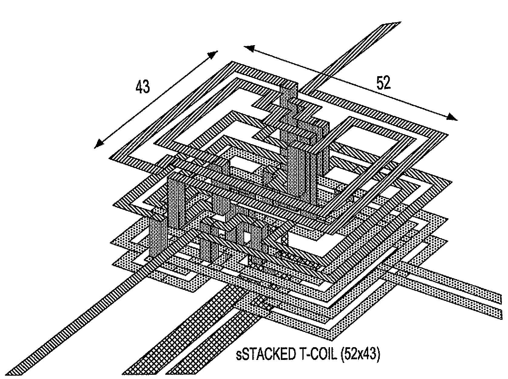
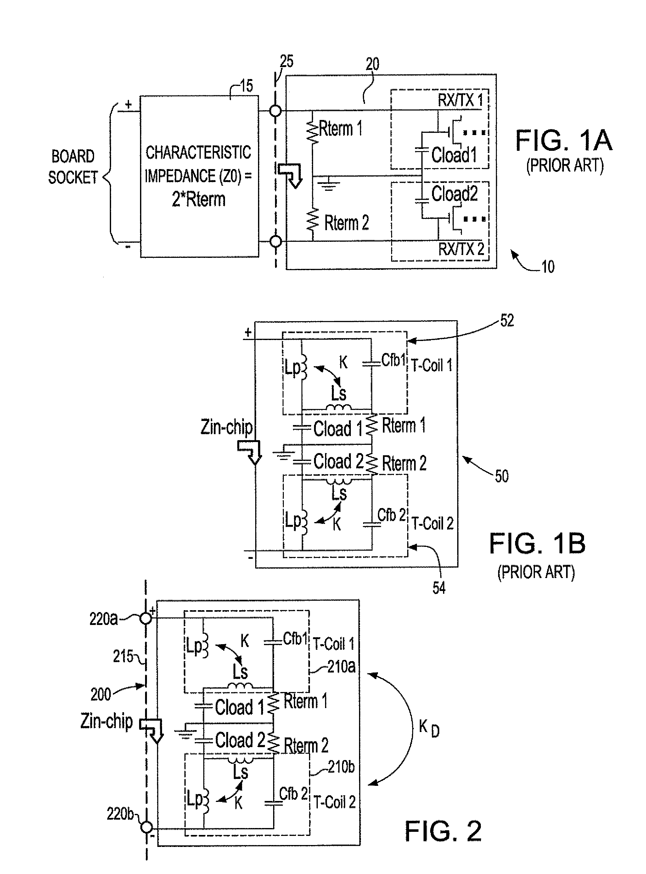
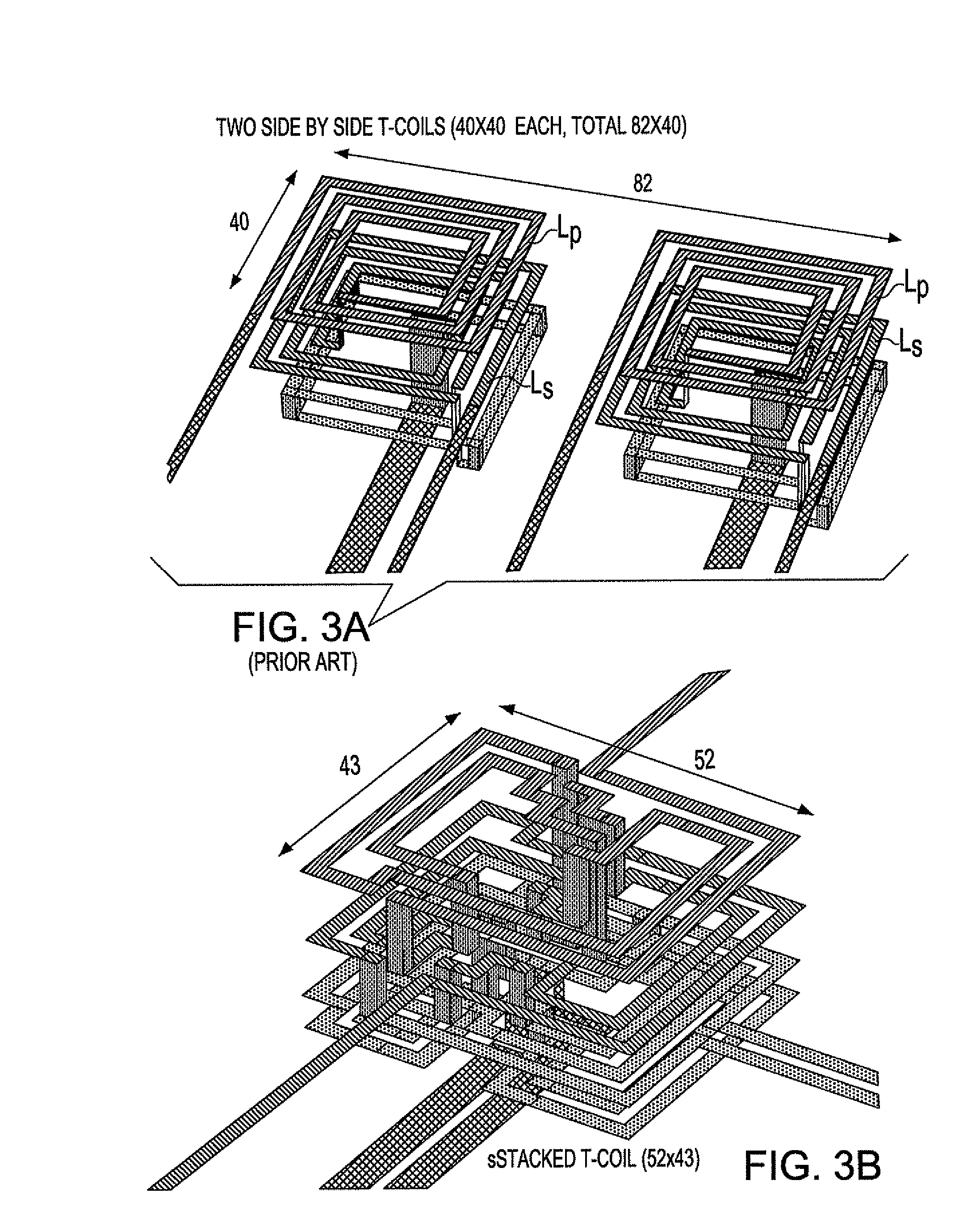
[0018]A first embodiment of the novel, stacked differential T-coil matching circuit 200 for use in an inventive IC system of the invention is shown in FIG. 2. Differential T-coil matching circuit 200 as shown in FIG. 2 is comprised of two stacked T-coils 210a, 210b, each of which are connected to an off-chip package interface 215 at plus and minus terminals, 220a, 220b, respectively. T-coils 210a, 210b, are shown functionally in their stacked relationship to include inherent primary and secondary inductances, LP and Ls, and inherent capacitance Cfb. The T-coils 210a, 210b, are each connected to individual termination resistors Rterm 1, Reterm2, and Cload1, Cload2, to ground, as shown. Arranging the two T-coils in the matching circuit as shown facilitates magnetic or field coupling between the proximate (stacked) T-coils during normal circuit and I / O channel operation. For that matter, the novel T-coils arrangement reduces required inductance for each T-coil by as much as one half, w...


PUM


Abstract

An integrated circuit (IC) system provides a broadband impedance matching function in a minimal IC area for operation with an external high-speed differential communications channel. The IC system includes a first semi-conductive substrate with a first face and an oppositely disposed second face substantially parallel to the first face. A second non-conductive substrate having substantially parallel first and second faces is arranged upon the first substrate so that the first face of the first substrate contacts the second face of the second substrate. An integrated semiconductor circuit (IC) is disposed in the first substrate and intended for differential high-speed communications operation with the external high-speed differential communications channel. First and second planar conductors are disposed in the second substrate to be electrically isolated from each other and from the first substrate, and arranged for maximum mutual magnetic additive coupling between them. The first terminal ends of the conductors present differential channel connections to the external differential communications channel that display an impedance at the circuit substantially equal to the external differential high-speed communications channel over a broad range of frequencies from DC to about 10 GHz.

Description

BACKGROUND OF THE INVENTION[0001]The present invention relates to high-speed communications applications, and more particularly relates to a differential T-coil impedance-matching circuit included in an integrated circuit (IC) system to match an impedance between the IC system's off-chip package (e.g., differential high-speed communications channel or circuit) and the on-chip circuitry required to interface and exchange data with the channel or off-chip package in a much reduced area within the IC comprising the IC system.[0002]High-speed I / O circuits require an effective impedance match between an off-chip package and the on-chip circuitry to ensure efficient power transfer and signal integrity, particularly during differential high-speed I / O circuit applications. The off-chip package, referred to interchangeably herein as channel, high-speed channel, differential high-speed channel, circuit and like expressions, typically behaves as a transmission line with a real characteristic i...

Claims


Application Information

Patent Timeline
Patent Type & Authority Patents(United States)
IPC IPC(8): H03H7/38
CPCH03H7/38H01F17/0013
Inventor GROVES, ROBERT A.
Owner IBM CORP
Why Eureka
Try Eureka