Electrostatic discharge protection

a technology of electrostatic discharge and protection, applied in the direction of semiconductor devices, semiconductor/solid-state device details, electrical apparatus, etc., can solve the problems of higher resistance, circuit to be protected is damaged before the thyristor and the resistance of the thyristor is reduced. , the effect of avoiding latching

Inactive Publication Date: 2008-12-30
INFINEON TECH AG
View PDF6 Cites 10 Cited by
  • Summary
  • Abstract
  • Description
  • Claims
  • Application Information

AI Technical Summary

Benefits of technology

[0015]In particular, the control occurs using a switch of the ESD protection device, by which the resistance that is present either between a first terminal of the thyristor, which can be connected to the first line, and a first point within the thyristor, or between a second terminal of the thyristor, which can be connected to the second line, and a second point within the thyristor, has a small resistance value when the switch is closed, and a high resistance value when the switch is open. Simultaneously, the ESD signal controls the base of a transistor that is present in the thyristor, in such a way that the ESD protection device is initiated. It is particularly advantageous that both the resistance and the base of the transistors are controlled only by the ESD signal. This makes compact implementation of the ESD protection device and reliable control of the ESD protection device possible.
[0016]Control is initiated by the ESD signal from the ESD protection device. In other words, an electrical connection between a specified (first or second) terminal of the thyristor and a specified (first or second) point within the thyristor is interrupted by the open switch, so that the resistance between the specified terminal and the specified point has a higher value than when the switch is closed. This change of the resistance value using the switch, which is, in particular, a transistor, is advantageously very robust and simple to implement.
[0019]By the switch (e.g., a transistor) being open in the ESD case, the resistance between the first terminal of the thyristor and the control input of the first transistor and the resistance between the first terminal of the thyristor and the collector of the second transistor are magnified compared with a state in which the switch is closed. Because a switch, such as a transistor, is simple to implement particularly in the case of semiconductor circuits, the ESD protection device according to the invention can be advantageously produced with only a very small surface overhead compared with a normal thyristor (without a switch), but nevertheless provides the advantages described above regarding improved conditions for becoming conductive and regarding the avoidance of latching compared with a normal thyristor (without a switch).
[0021]Additionally, there is an embodiment in which the ESD protection device includes a control device that captures the ESD case between the first and second lines, and is thus able to generate the ESD signal. Advantageously, consequently in the case of this embodiment, the ESD signal does not have to be fed to the ESD protection device.
[0023]The ESD protection arrangement is thus able to divert a surge which occurs on any of the first lines which are assigned to the ESD protection arrangement via the appropriate ESD protection device which is connected to this first line.
[0029]The ESD protection system according to the invention is thus able to capture the ESD case which occurs between any one of the first lines and the second line, and to divert it via at least one ESD protection arrangement, which, as explained, may also be an ESD protection device. To protect a circuit from surges, the ESD protection system can be in such a form that the ESD protection arrangements and ESD protection devices, and the control devices if any, are arranged somewhere within the circuit to be protected, so that the ESD protection system can be advantageously and flexibly constructed.

Problems solved by technology

There may be two problems in prior art thyristor circuits.
First, they often have a very high switching voltage 24, with the result that the circuit to be protected is damaged before the thyristor reaches the conducting state region (region in which the thyristor 1 has low resistance).
If the voltage that is present at the thyristor 1, which is operated in the conducting state region, does not fall below the holding voltage, the thyristor 1 remains in the conducting state region, which is undesirable because malfunctions or even destruction of a circuit to be protected may occur.
The second problem is particularly disadvantageous circuits that are operated at 3 to 5 V or higher and are to be protected.
However, these approaches result in a higher resistance when the thyristor is operated in the conducting state region, which is disadvantageous for the circuit to be protected, since a higher current then flows through the circuit in the ESD case.
However, this approach has the disadvantage that the thyristor in ESD cases with small or even medium voltage swings does not fire, so that there is insufficient protection for the circuit to be protected.
There are also certain circuits to be protected where the system requirements do not limit a maximum current value, for which reason this solution approach cannot be carried out for these circuits.

Method used


Image

  • Electrostatic discharge protection
  • Electrostatic discharge protection
  • Electrostatic discharge protection

Examples


Embodiment Construction

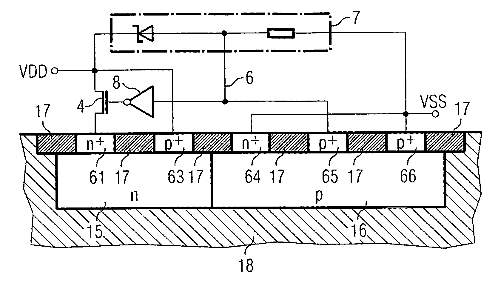
[0045]FIG. 4a represents an ESD protection device 19 that diverts an electrostatic discharge between a first terminal 27 and a second terminal 28 of the ESD protection device 19, the potential of the first terminal 27 being higher than the potential of the second terminal 28 (for instance, the first terminal 27 can be connected to VDD and the second terminal 28 to VSS). The first terminal 27 is connected to the emitter of a PNP transistor 25, and via an NMOS transistor 4 and an n-well resistor 11 to the base of the PNP transistor 25 and the collector of an NPN transistor 26. The collector of the PNP transistor 25 is connected to the base of the NPN transistor 26, to an ESD signal 6 and via a p-well resistor 12 to the second terminal 28. The emitter of the NPN transistor 26 is also connected to the second terminal 28. The ESD signal 6 that is inverted via an inverter 8 controls the NMOS transistor 4. A contact point 13 in front of the base of the PNP transistor 25 is called the n-wel...


PUM


Abstract

An electrostatic discharge (“ESD”) protection device, which includes a thyristor circuit, in the ESD case increases a resistance of the ESD protection device in comparison with a non-ESD case, by means of a switch. An ESD protection arrangement may include a ESD protection device to protects circuits with multiple voltage potentials. An ESD protection system may also include an ESD protection arrangement, to which an ESD signal is fed via a bus of the ESD protection system. The ESD protection device and ESD protection arrangement, and thus the ESD protection system, can be provided in a compact semiconductor arrangement.

Description

PRIORITY AND CROSS REFERENCE TO RELATED APPLICATION[0001]This application claims priority to German Patent Application No. 10 2005 000 801.1, filed Jan. 5, 2005, entitled DEVICE, ARRANGEMENT AND SYSTEM FOR ESD PROTECTION, which is incorporated in its entirety herein by reference.BACKGROUND OF THE INVENTION[0002]1. Field of the Invention[0003]The present invention relates to an electrostatic discharge (“ESD”) protection device, an ESD protection arrangement and an ESD protection system, to protect a micro-electronic circuit or semiconductor circuit from electrostatic discharge. This invention also relates to a semiconductor circuit having the ESD protection device, the ESD protection arrangement or the ESD protection system.[0004]2. Description of the Related Art[0005]Controllable rectifiers, or thyristors, are used for protection from electrostatic discharges (the ESD case). An advantage of thyristors is that they support a high current density before damage to the thyristor occurs ...

Claims


Application Information

Patent Timeline
Patent Type & Authority Patents(United States)
IPC IPC(8): H01L27/12H01L31/0392
CPCH01L27/0262
Inventor GOSSNER, HARALD
Owner INFINEON TECH AG
Why Eureka
Try Eureka