Specimen current mapper

a current mapper and current technology, applied in the direction of semiconductor/solid-state device testing/measurement, instruments, nuclear engineering, etc., can solve problems such as process yield loss

Inactive Publication Date: 2009-01-06
APPL MATERIALS ISRAEL LTD
View PDF32 Cites 8 Cited by
  • Summary
  • Abstract
  • Description
  • Claims
  • Application Information

AI Technical Summary

Benefits of technology

[0008]It is an object of some aspects of the present invention to provide improved methods and systems for monitoring production of contact openings.
[0009]In embodiments of the present invention, contact openings on a sample, typically a semiconductor wafer, are irradiated at multiple locations with a focused beam of charged particles, along a beam axis that deviates substantially in angle from a normal to the surface of the sample. At each location, the specimen current is measured and recorded, along with coordinate information. The specimen current measurements over the entire sample, or a region of the sample, are mapped in graphical or in numerical form. The map facilitates detection of deviations of the measured specimen current from benchmark values and of process non-uniformities over the sample that cause uneven etching of the contact openings.
[0010]The measured specimen current at each location serves as a quantitative measure of the quality of contact openings at the location. Specimen current magnitude can serve as a measure of the thickness of the residue on the bottom of a contact opening. Typically, a high absolute value of the specimen current indicates good contact to ground, while low absolute value indicates higher resistance to ground. The use of an angled beam of charged particles to irradiate the sample provides enhanced sensitivity to thin residue layers that may remain at the bottom of contact openings. The combination of angling the beam and mapping the resultant specimen current thus provides a particularly sensitive, integrated picture of the accuracy and uniformity of the process that is used to create the contact openings.

Problems solved by technology

If these variations are too large, they impact on device performance and can lead to loss of process yield.

Method used


Image

  • Specimen current mapper
  • Specimen current mapper
  • Specimen current mapper

Examples


Embodiment Construction

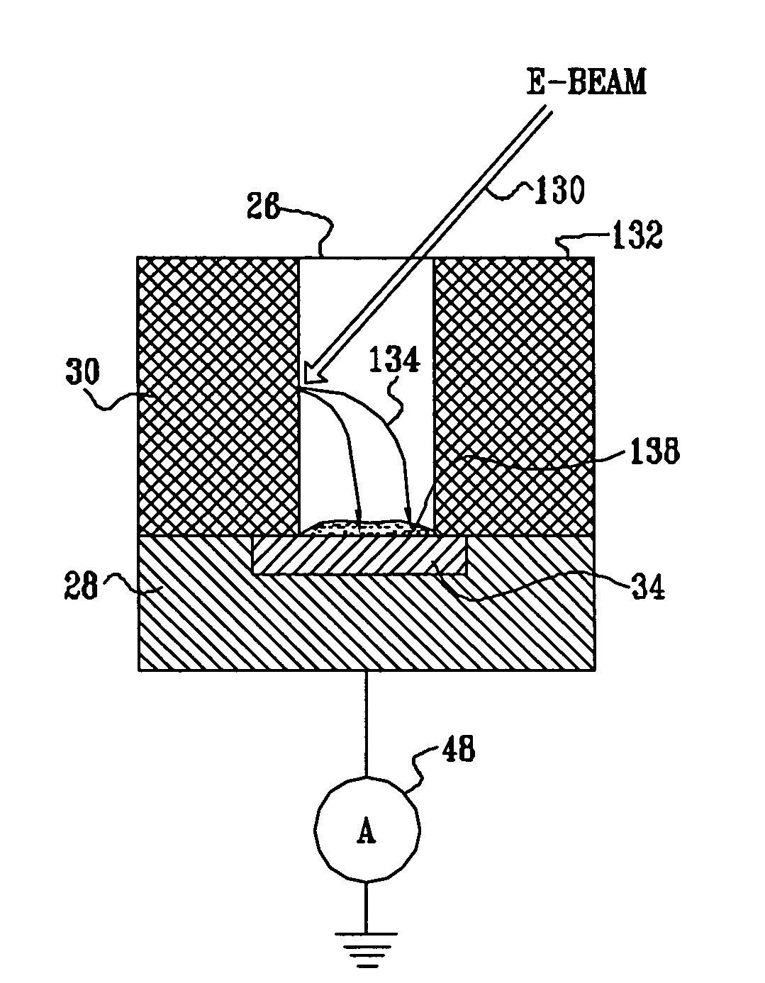
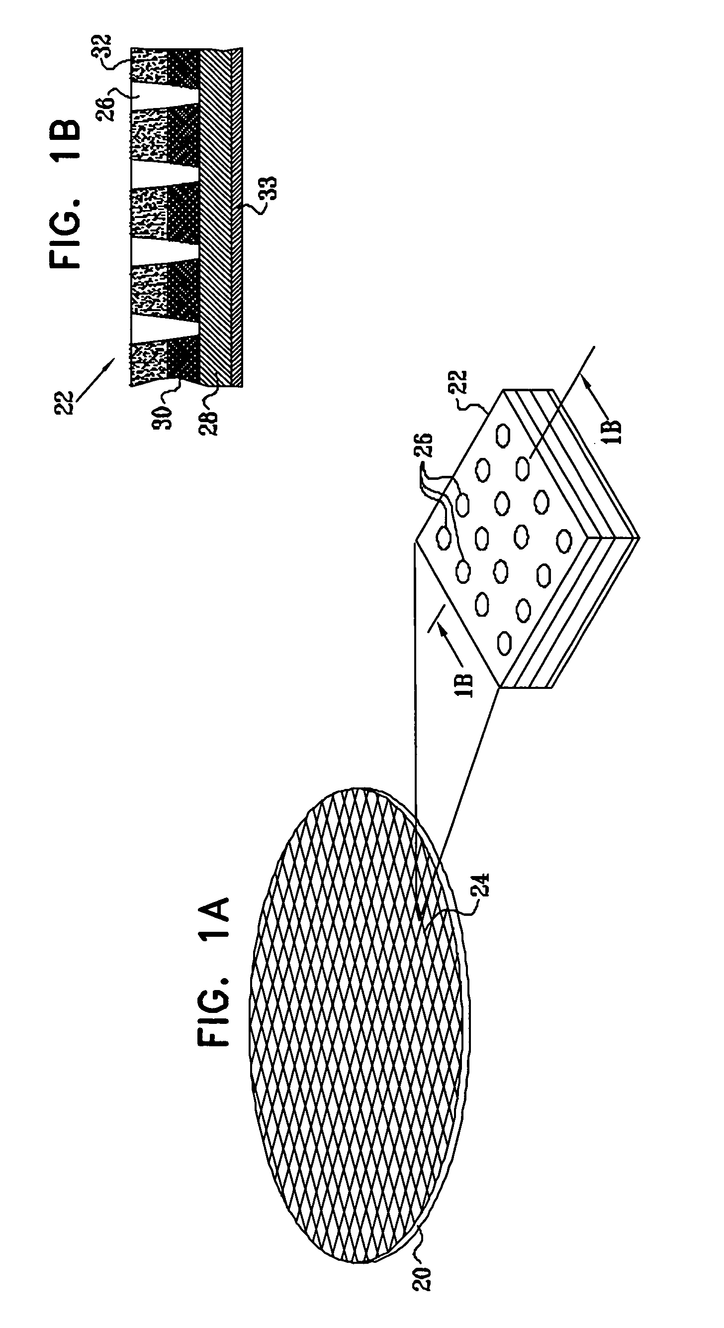
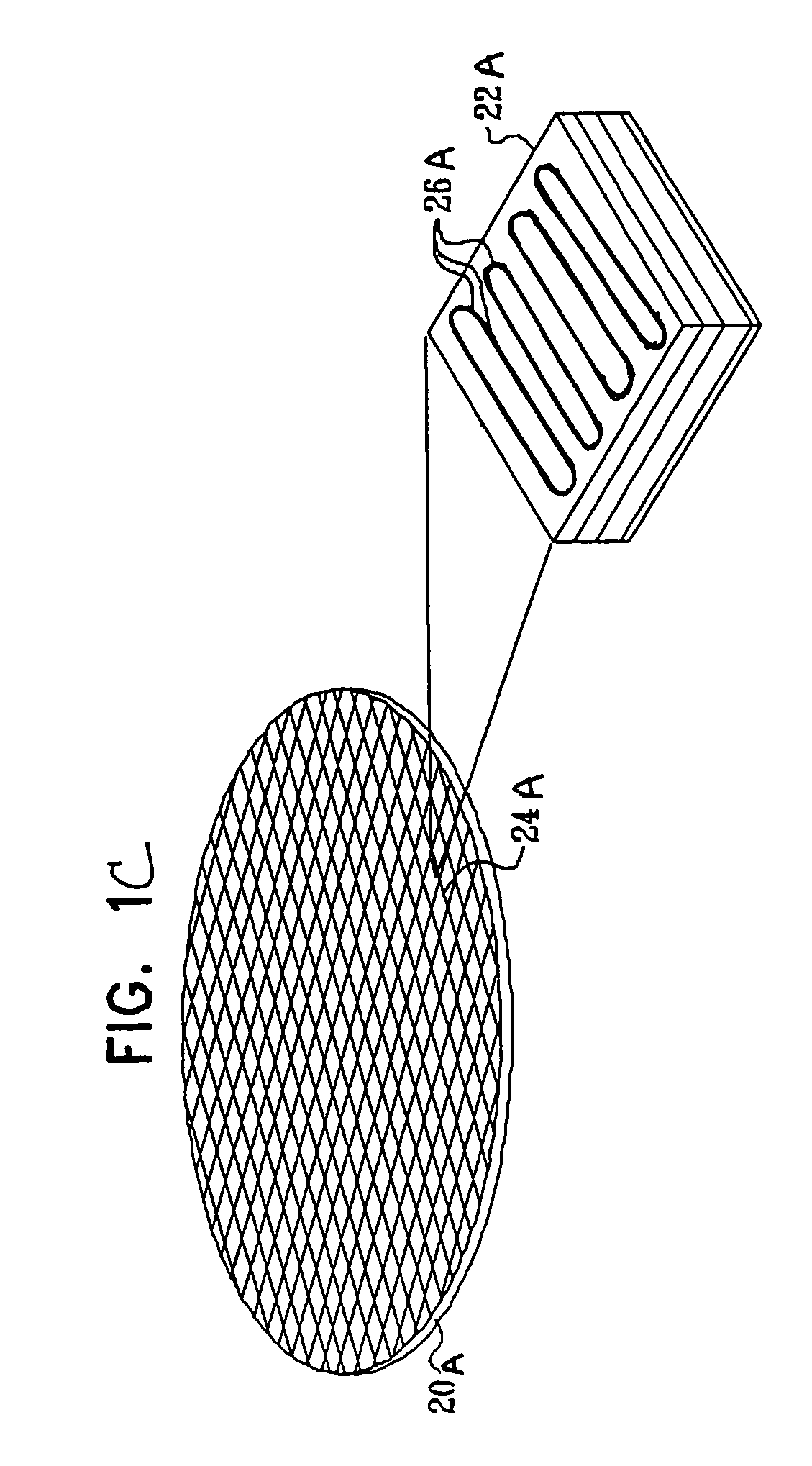
[0051]Reference is now made to FIGS. 1A and 1B, which schematically illustrate a semiconductor wafer 20 and details of a pattern 22 of contact holes 26 formed thereon, in accordance with an embodiment of the present invention. FIG. 1A is a top view of the wafer, with the pattern shown enlarged in an inset. FIG. 1B is an enlarged, cross-sectional view of the pattern, taken along line 1B-1B in FIG. 1A. Pattern 22 may be a dedicated test pattern, for use in specimen current mapping, as described below, or it may compnse a group of production contact holes in a known location on wafer 20. (Exemplary test patterns are described in the above-mentioned U.S. patent application Ser. No. 10 / 209,087.) Although only the single pattern 22 is shown in FIG. 1A by way of example, multiple patterns of this sort, distributed over the surface of wafer 20, are used in specimen current mapping. The pattern may also include other types of contact openings, such as trenches or vias. A pattern 22A of trenc...


PUM


Abstract

A method for process monitoring includes receiving a sample having a first layer that is at least partly conductive and a second layer formed over the first layer, following production of contact openings in the second layer. A beam of charged particles is directed along a beam axis that deviates substantially in angle from a normal to a surface of the sample, so as to irradiate one or more of the contact openings in each of a plurality of locations distributed over at least a region of the sample. A specimen current flowing through the first layer is measured in response to irradiation of the one or more of the contact openings at each of the plurality of locations. A map of at least the region of the sample is created, indicating the specimen current measured in response to the irradiation at the plurality of the locations.

Description

CROSS-REFERENCE TO RELATED APPLICATIONS[0001]This application is a continuation in part of allowed U.S. patent application Ser. No. 10 / 434,977, filed 9 May 2003, now U.S. Pat. No. 7,038,224, which is a continuation in part of U.S. patent application Ser. No 10 / 209,087filed 30 Jul. 2002 now U.S. Pat. No. 7,078,690. The disclosures of these related applications are incorporated herein by reference.FIELD OF THE INVENTION[0002]The present invention relates generally to semiconductor device manufacturing and process control, and specifically to monitoring of process quality and uniformity.BACKGROUND OF THE INVENTION[0003]Contact hole production is a common step in semiconductor device manufacturing. The contact holes are typically used to make electrical connections to a semiconductor or metal layer through an overlying non-conducting (dielectric) layer, such as an oxide layer. In order to produce contact holes, a layer of photoresist is first deposited on the wafer surface. The photores...

Claims


Application Information

Patent Timeline
Patent Type & Authority Patents(United States)
IPC IPC(8): H01J49/44H01L21/00H01L21/66H01L23/544
CPCH01J37/32935H01L22/34H01J2237/281H01J2237/2815H01L21/67253H01L22/12H01L2924/3011
Inventor KADYSHEVITCH, ALEXANDERSHEMESH, DRORBRAMI, YANIVSHUR, DMITRY
Owner APPL MATERIALS ISRAEL LTD
Why Eureka
Try Eureka