Circuit arrangement and method for driving a gate of a transistor, in particular a MOSFET

a transistor and gate technology, applied in the direction of pulse technique, motor/generator/converter stopper, dynamo-electric converter control, etc., can solve the problems of relatively high losses in the overall embodiment of an electronic device, increased power loss at all dimming settings,

Inactive Publication Date: 2009-01-06
OSRAM GMBH
View PDF2 Cites 2 Cited by
  • Summary
  • Abstract
  • Description
  • Claims
  • Application Information

AI Technical Summary

Benefits of technology

[0008]The present invention is therefore based on the object of providing a circuit arrangement and a method for driving a gate of a transistor, with which circuit arrangement and with which method it is possible to overcome the disadvantages of the prior art. In particular, the intention is to achieve a situation in which an improved EMI response can be ensured at all dimming settings and an appropriate adjustment of the power loss can be achieved.
[0009]A circuit arrangement according to the invention is designed for driving a gate of a transistor, which is, in particular, a MOSFET, the transistor being arranged in an electronic device. One essential concept of the invention consists in the fact that the circuit arrangement is designed for variably driving the gate of the transistor as a function of the operating state of the electronic device, in which the transistor is used. This makes it possible to achieve a situation in which the power loss can be altered or influenced individually and precisely and losses now only need to be increased in the region in which they are required. The invention can be used to optimize the EMI response at all dimming settings in particular when the circuit arrangement according to the invention is arranged in an electronic ballast. Variable driving of the gate as a function of the operating state of the electronic device makes it possible to set the power loss at all dimming settings depending on the situation and therefore in an efficient and effective manner.
[0010]The circuit arrangement advantageously comprises a control unit, which is designed for variably driving the gate of the transistor, the circuit arrangement furthermore also having a gate driver circuit, which can be electrically connected to the control unit (low-side driver) or else has electrical isolation—magnetic or optical or capacitive—for the purpose of driving an upper transistor in a half-bridge arrangement (high-side driver) and can be parameterized by the control unit, the gate driver circuit being electrically connected to the gate of the transistor. The implementation of the circuit arrangement according to the invention is thus relatively low in complexity and has a space-saving design.
[0015]In one method according to the invention for driving a gate of a transistor, which is in particular in the form of a MOSFET, and in which the transistor is arranged in an electronic device, the gate of the transistor is driven in variable fashion as a function of the operating state of this electronic device. The method according to the invention can thus make it possible for a power loss to be altered, as required, and only to be altered in situations in which this is necessary. Furthermore, with the method according to the invention, which is advantageously carried out in an electronic ballast, it is possible to achieve a situation in which the EMI response can be positively influenced at all dimming settings when setting dimming settings of the electronic ballast. With the method according to the invention, which is carried out in an electronic ballast, it is thus also possible to achieve a situation in which the power loss at all dimming settings can be adjusted, in particular increased, effectively and efficiently as a function of the correspondingly present situation.

Problems solved by technology

One significant disadvantage with such a procedure, however, is the fact that the power loss is increased at all dimming settings.
This in turn leads to relatively high losses in the overall embodiment of an electronic device, in which such a MOS transistor having such a drive circuit is arranged.

Method used


Image

  • Circuit arrangement and method for driving a gate of a transistor, in particular a MOSFET
  • Circuit arrangement and method for driving a gate of a transistor, in particular a MOSFET
  • Circuit arrangement and method for driving a gate of a transistor, in particular a MOSFET

Examples


Embodiment Construction

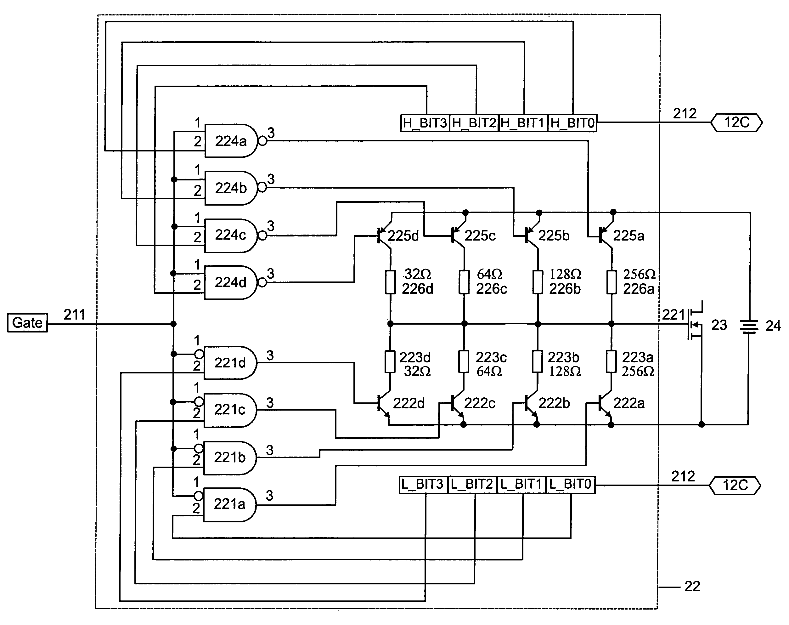
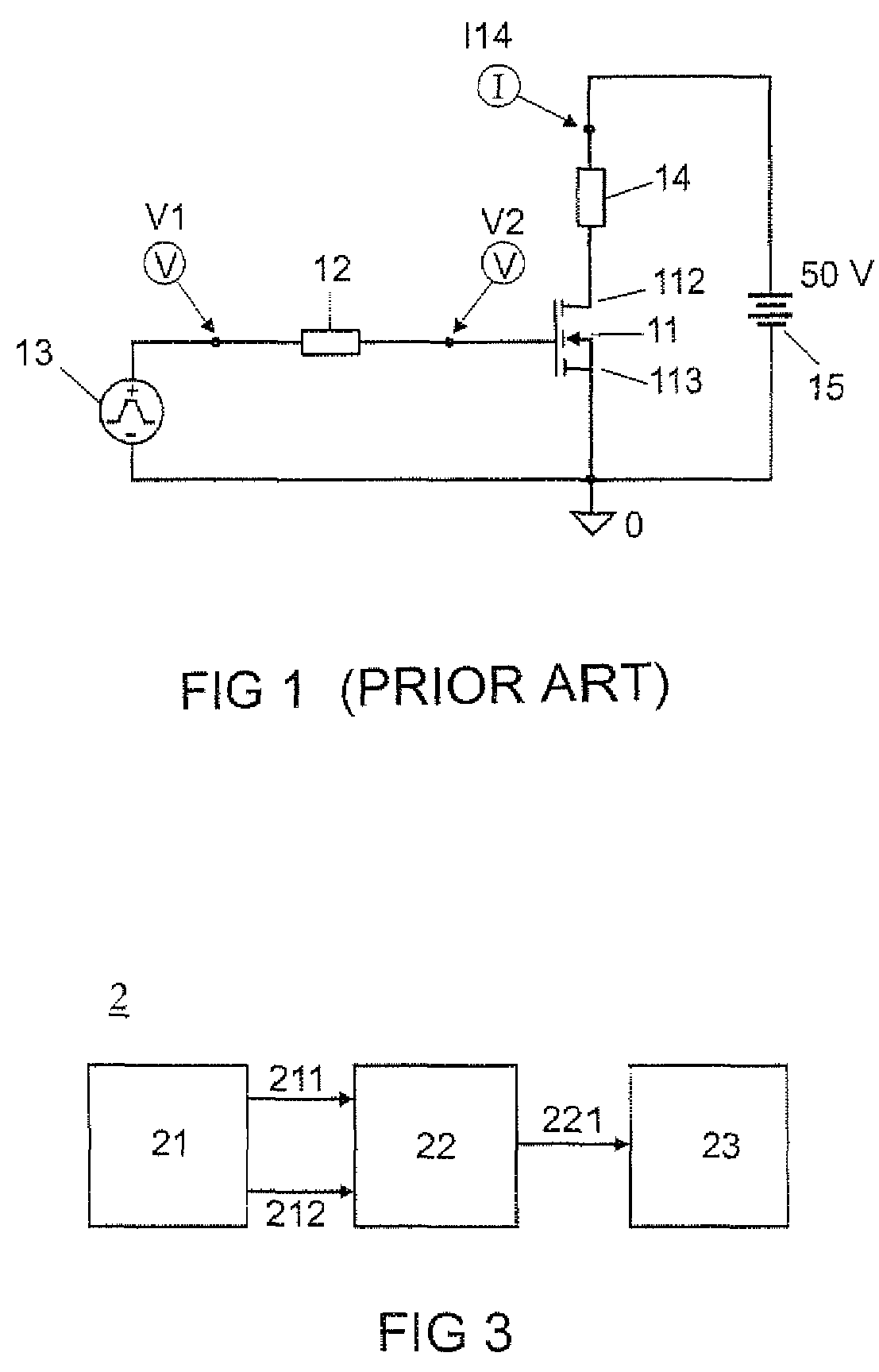
[0021]FIG. 3 shows a simplified block circuit diagram of a circuit arrangement 2 according to the invention. The circuit arrangement 2 comprises a control unit, which in the exemplary embodiment is in the form of a microprocessor 21. Furthermore, the circuit arrangement 2 comprises a gate driver circuit 22. As can be seen from the illustration in FIG. 3, the microprocessor 21 is electrically connected to the gate driver circuit 22, the microprocessor 21 being designed for transmitting a gate driving signal 211. The microprocessor 21 is designed for transmitting a parameterization signal 212 to the gate driver circuit 22 via a further signal connection formed in the exemplary embodiment. The gate driver circuit 22 is connected to a transistor, which in the exemplary embodiment is in the form of a MOSFET 23. The electrical connection of the gate driver circuit 22 is in this case formed in particular to send a signal 221 to the gate of the MOSFET 23.

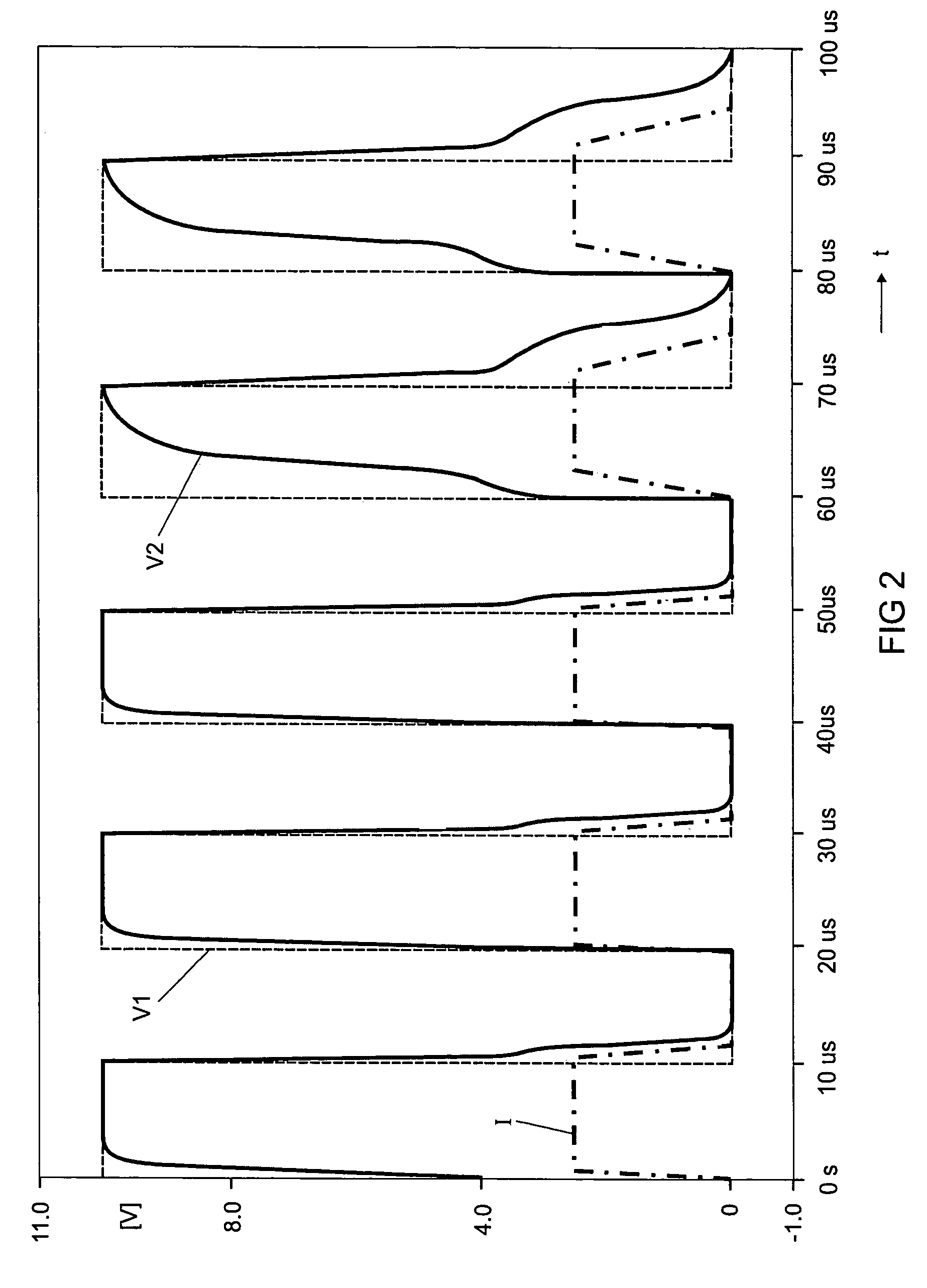
[0022]As can already be seen in the ...


PUM


Abstract

The present invention relates to a circuit arrangement for driving a gate of a transistor, in particular a MOSFET, which is arranged in an electronic ballast, the circuit arrangement (2) being designed for the variable driving of the gate (221) as a function of the operating state of the electronic ballast. The invention also relates to a method for driving a gate of such a transistor.

Description

BACKGROUND OF THE INVENTION[0001]1. Field of the Invention[0002]The present invention relates to a circuit arrangement for driving a gate of a transistor, in particular a MOSFET. The invention also relates to a method for driving a gate of such a transistor.[0003]2. Description of the Related ArtPrior Art[0004]Circuit arrangements for driving gates of transistors are known. Such a known circuit arrangement is illustrated in FIG. 1. The circuit arrangement 1 comprises a MOS transistor 11, which is electrically connected with its gate 111 to a gate series resistor 12. The gate series resistor 12 is electrically connected to a pulsed DC voltage source 13. As can further be seen in FIG. 1, the drain terminal 112 of the MOS transistor 11 is connected to a load resistor 14, this load resistor 14 being electrically connected to a voltage source 15. Furthermore, the source terminal 113 of the MOS transistor 11 is connected to ground potential. The circuit arrangement 1 illustrated in FIG. 1...

Claims


Application Information

Patent Timeline
Patent Type & Authority Patents(United States)
IPC IPC(8): G05F1/40
CPCH03K17/163H03K2217/0036
Inventor LOTT, JORG
Owner OSRAM GMBH
Why Eureka
Try Eureka