Nitride semiconductor light emitting device

a light-emitting device and semiconductor technology, applied in the direction of semiconductor devices, basic electric elements, electrical equipment, etc., can solve the problems of reducing the effective area of light-emitting, low light-emitting efficiency per light-emitting area, and limited light-emitting efficiency, so as to improve the current spreading effect, enhance electron mobility, and increase the concentration of sheet carriers

Active Publication Date: 2009-01-20
SAMSUNG ELECTRONICS CO LTD
View PDF2 Cites 4 Cited by
  • Summary
  • Abstract
  • Description
  • Claims
  • Application Information

AI Technical Summary

Benefits of technology

[0011]The present invention has been made to solve the foregoing problems of the prior art and it is therefore an object of the present invention to provide a high-efficient nitride semiconductor light emitting device with excellent current spreading effect by forming an appropriate two-dimensional electronic gas layer (2DEG) in an n-type nitride area to increase sheet carrier concentration and enhance electron mobility.
[0013]This allows formation of the 2DEG layer on the AlxGa1-xN (0<x<1) layer, resulting in higher electron mobility and thus uniform current spreading.
[0016]The AlN layer employed in the invention generates a beneficial piezoelectric effect for increasing electron concentration of the 2 DEG layer. Also, the AlN layer blocks dislocation as an insulation layer and boosts current spreading effect further. To achieve such effect properly, preferably, the AlN layer has a thickness of about 5 Å to 30 Å.
[0020]In a specific embodiment of the invention, the nitride semiconductor light emitting device further comprises a high-resistant GaN layer formed between the first n-type GaN layer and the AlxGa1-xN layer, where impurities are intentionally undoped, wherein the two-dimensional electron gas layer is formed at an interface of the high-resistant GaN layer. In this case, the high-resistant GaN layer additionally boosts current spreading effect. Preferably, the high-resistant GaN layer has a thickness of 80 Å to 200 Å.

Problems solved by technology

Compared to a vertical light emitting device having two electrodes on opposed faces of the light emitting structure, the planar nitride light emitting device is disadvantaged in that an effective area for light emitting is not large-sized due to non-uniform current distribution across the light emitting area and thus light emitting efficiency per light-emitting area is low. FIG. 1 explains the planar light emitting device and limited light emitting efficiency thereof.
Disadvantageously, this reduces an effective area for light emitting.
In addition, current crowding causes a great amount of current to be applied in case of a temporary spark or overload.
Consequently, heat generated at this time renders the device easily breakable, and thus weakly resistant to electrostatic discharge (ESD).

Method used


Image

  • Nitride semiconductor light emitting device
  • Nitride semiconductor light emitting device
  • Nitride semiconductor light emitting device

Examples


Embodiment Construction

[0028]Preferred embodiments of the present invention will now be described in detail with reference to the accompanying drawings.

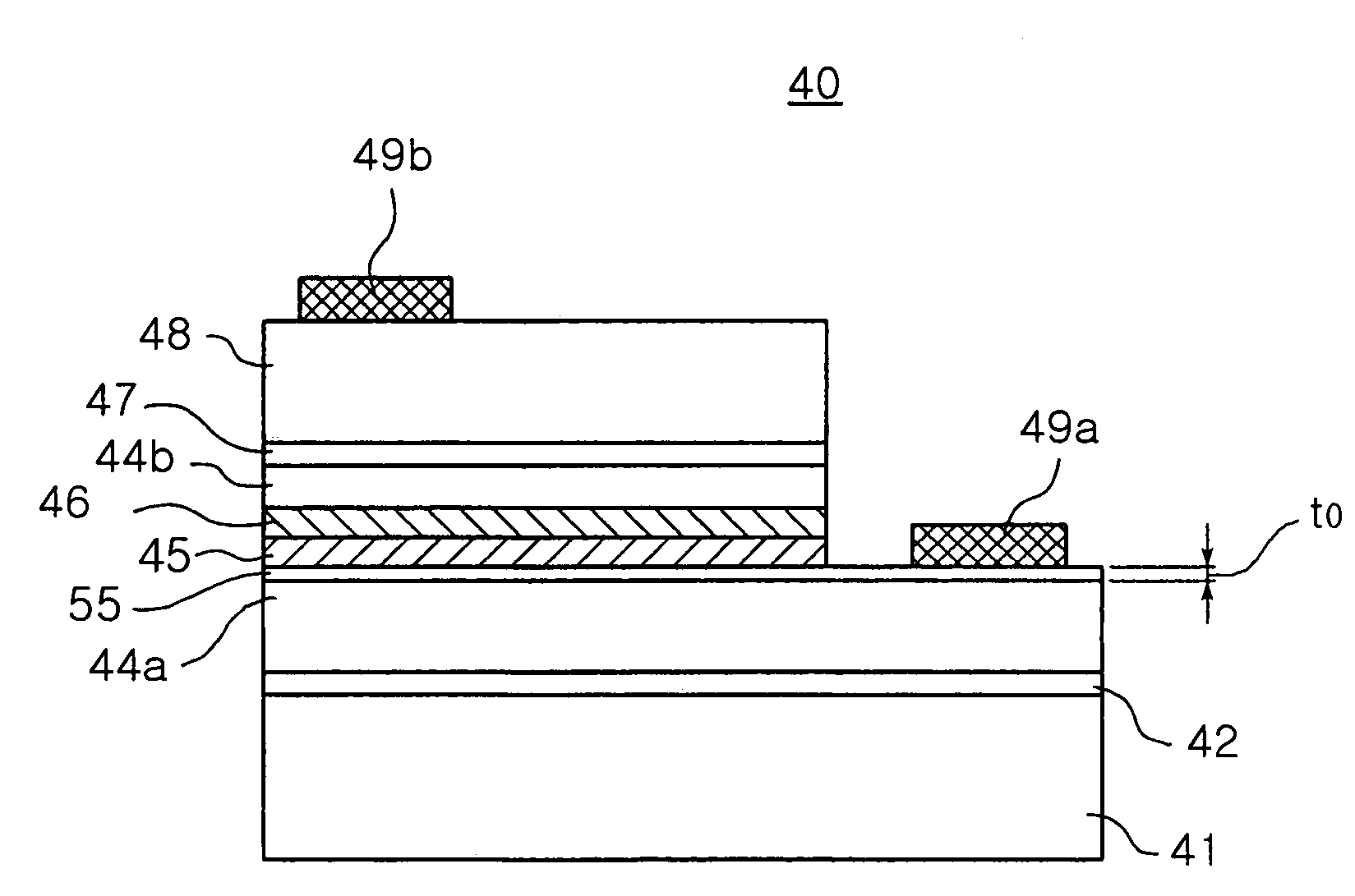
[0029]FIG. 2 is a vertical cross-sectional view illustrating a nitride semiconductor light emitting device according to one embodiment of the invention.

[0030]First, referring to FIG. 2, the nitride semiconductor light emitting device 20 according to this embodiment includes a sapphire substrate 21, a buffer layer 22 formed on the sapphire substrate 21, n-type nitride semiconductor layers 24a and 24b formed on the buffer 22, an active layer 27 formed on the n-type nitride semiconductor layer 24b and a p-type nitride semiconductor layer 28 formed on the active layer 27. An n-electrode 29a and a p-electrode 29b are disposed to connect to the n- and p-type nitride semiconductor layers, respectively.

[0031]The n-type nitride semiconductor layers include a first n-type GaN layer 24a and a second n-type GaN layer 24b in the order of distance from the active layer ...


PUM


Abstract

The invention provides a nitride semiconductor device and a manufacturing method thereof. In the invention, n-type and p-type nitride semiconductor layers are formed on a substrate, and an active layer is formed therebetween. The n-type nitride semiconductor layers include first and second n-type GaN layers disposed in the order of distance from the active layer. In addition, in the nitride semiconductor device of the invention, an AlxGal-xN layer, where 0<x<1, is interposed between the first and second n-type GaN layers, thereby forming a two-dimensional electron gas layer at interfaces of the first and second n-type GaN layers.

Description

CLAIM OF PRIORITY[0001]This application claims the benefit of Korean Patent Application No. 2005-42090 filed on May 19, 2005 in the Korean Intellectual Property Office, the disclosure of which is incorporated herein by reference.BACKGROUND OF THE INVENTION[0002]1. Field of the Invention[0003]The present invention relates to a nitride semiconductor light emitting device, more particularly to a high brightness nitride semiconductor light emitting device improved in current spreading effect via a novel heterogeneous bonding structure.[0004]2. Description of the Related Art[0005]In general, a nitride semiconductor layer is a group III-V semiconductor crystal such as GaN, InN, and AlN, which is broadly utilized in a light emitting device capable of generating light of short wavelength (ultraviolet rays or green light), especially blue light. The nitride semiconductor light emitting device is fabricated with an insulating substrate such a sapphire substrate or a SiC substrate which satisf...

Claims


Application Information

Patent Timeline
Patent Type & Authority Patents(United States)
IPC IPC(8): H01L33/00H01L33/14H01L33/32
CPCH01L33/14H01L33/32
Inventor LEE, JAE HOONCHOI, HEE SEOKOH, JEONG TAKLEE, SU YEOL
Owner SAMSUNG ELECTRONICS CO LTD
Why Eureka
Try Eureka