Producing a frequency-representative signal with rapid adjustment to frequency changes

Active Publication Date: 2009-01-20
NAT SEMICON CORP
11 Cites 5 Cited by

AI-Extracted Technical Summary

Problems solved by technology

This locking time can present difficulties in some situations, for example, when...

Method used

[0019]As shown in FIG. 4, the output current Iout drives a capacitor C4 which is used in combination with the feed-back path 15 to increase the accuracy of the output current Iout. Note, however, that the o...

Abstract

A feed-forward path is combined with a feed-back path to produce an output signal representation of an input signal frequency. The feed-forward path adjusts the output signal representation in response to a change in the input signal frequency, and does so in a response time that is independent of the feed-back path. Input frequencies can be represented as voltages, and first and second input frequency ranges which differ from one another can both be represented in the same range of voltages.

Application Domain

Differential amplifiersOscillations comparator circuits +3

Technology Topic

Voltage rangeSignal frequency +1

Image

  • Producing a frequency-representative signal with rapid adjustment to frequency changes
  • Producing a frequency-representative signal with rapid adjustment to frequency changes
  • Producing a frequency-representative signal with rapid adjustment to frequency changes

Examples

  • Experimental program(1)

Example

[0012]FIGS. 1 through 5, discussed herein, and the various embodiments used to describe the principles of the present invention in this patent document are by way of illustration only and should not be construed in any way to limit the scope of the invention. Those skilled in the art will understand that the principles of the present invention may be implemented in any suitably arranged system.
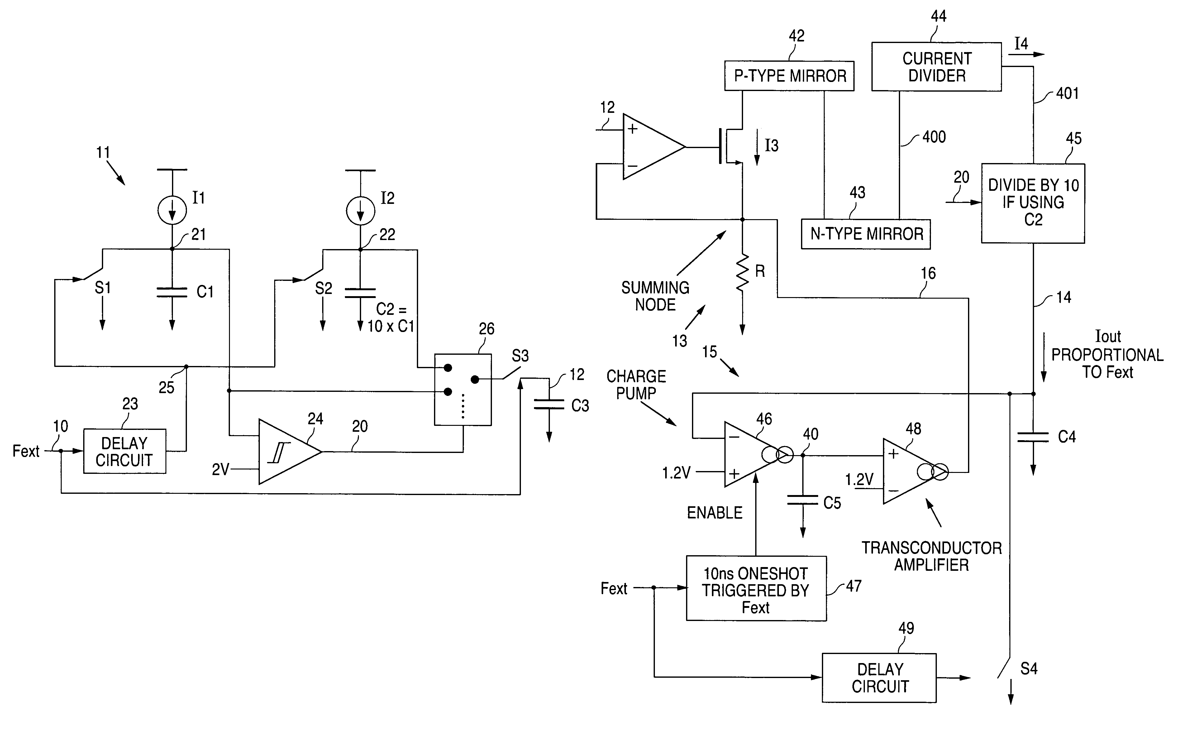
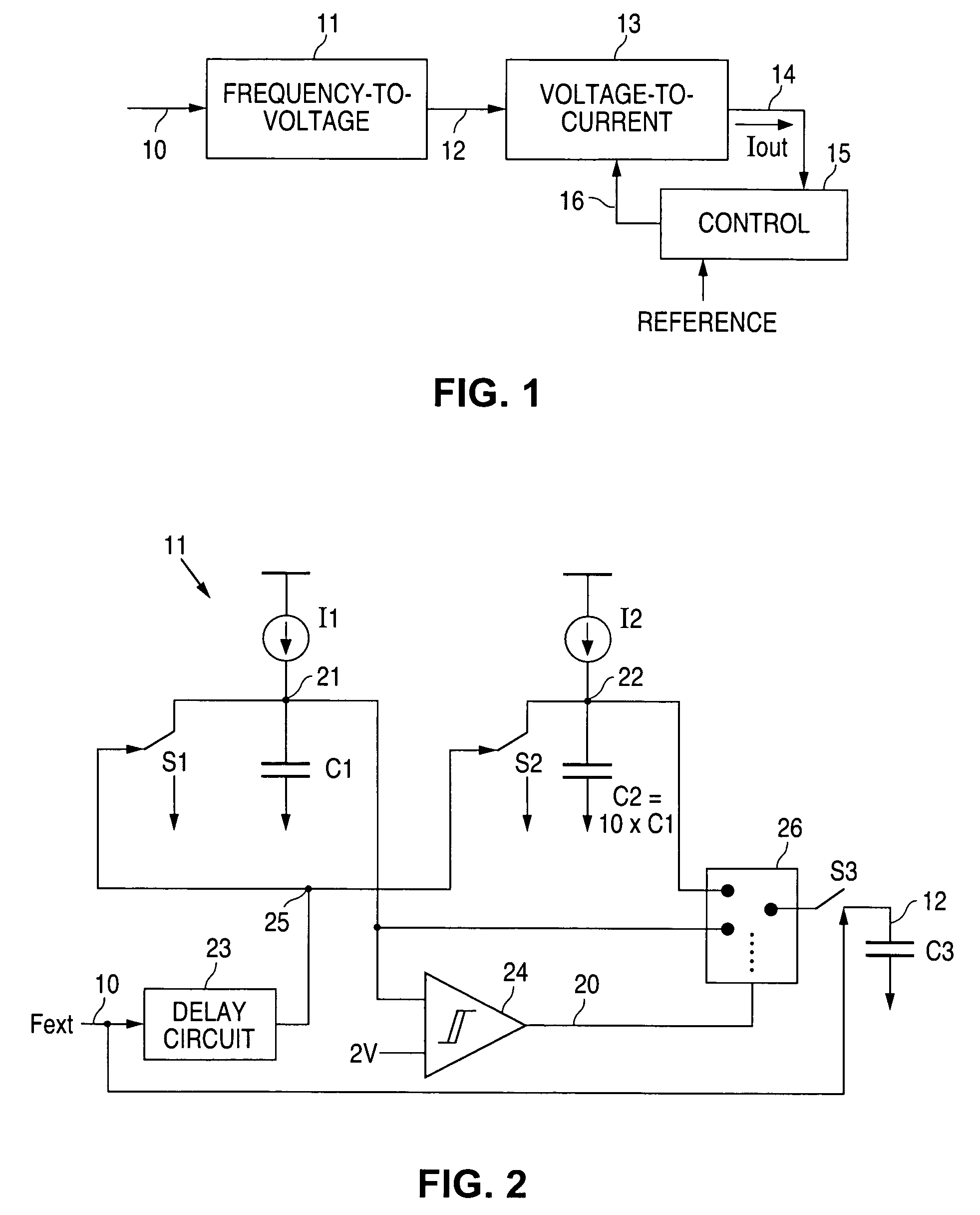
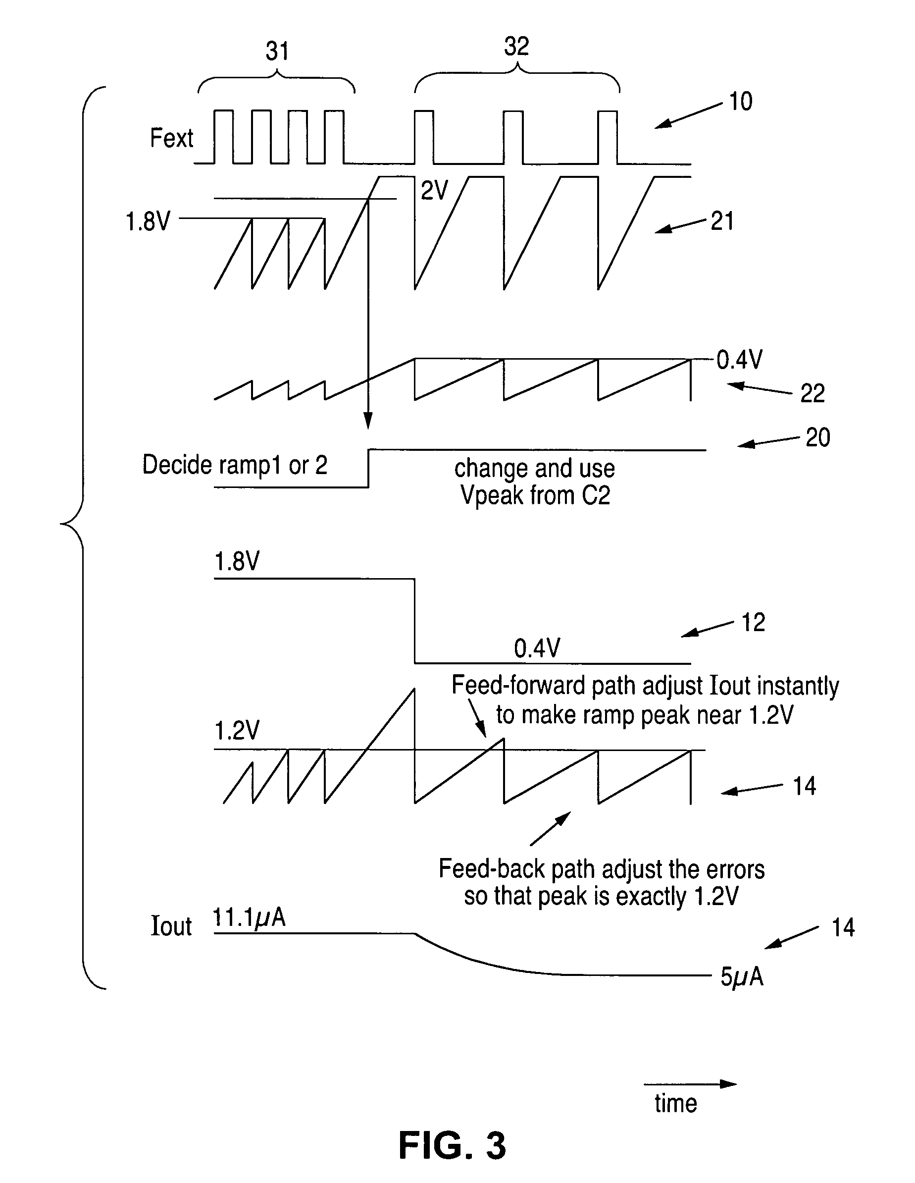
[0013]FIG. 1 diagrammatically illustrates a frequency-to-current conversion apparatus according to exemplary embodiments of the invention. The apparatus of FIG. 1 includes a frequency-to-voltage converter 11 which produces at 12 an output voltage that represents the frequency of an input signal received at 10. In response to the voltage at 12, a voltage-to-current converter 13 produces at 14 an output current Iout that represents the frequency of the input signal received at 10. A feed-back control path (or loop) at 15 provides feed-back control signaling between the output 14 of the voltage-to-current converter 13 and another node 16 of the voltage-to-current converter 13. The feed-back control path 15 provides adjustment capability, but the combination of the frequency-to-voltage converter 11 and the voltage-to-current converter 13 represents a feed-forward path which permits the output 14 to adjust immediately to frequency changes at the input 10. As described in detail herein below, this feed-forward adjustment can be accomplished without incurring any time delay associated with operation of the feed-back control path 15.
[0014]FIG. 2 illustrates the frequency-to-voltage converter 11 of FIG. 1 in more detail according to exemplary embodiments of the invention. The frequency-to-voltage converter 11 of FIG. 2 includes a first frequency-to-voltage conversion circuit including a current source I1 coupled in series with a parallel combination of a switch S1 and a capacitor C1. Similarly, a second frequency-to-voltage conversion circuit includes a current source I2 coupled in series with a parallel combination of a switch S2 and a capacitor C2. The switches S1 and S2 are controlled by a delayed version 25 of the input frequency Fext, which delayed version 25 is produced by a suitable delay circuit 23. The input frequency Fext also controls a switch S3 that is connected between a selector 26 and a sample/hold capacitor C3 (C3 1, C3 2) at the output 12 of the frequency-to-voltage converter 11. The selector 26 has a first input connected to a node 21 of the first frequency-to-voltage conversion circuit, and has a second input connected to a node 22 of the second frequency-to-voltage conversion circuit. Under control of the output 20 of a comparator 24, the selector 26 connects one of the nodes 21 and 22 to the switch S3. The comparator 24 compares the voltage at the node 21 to a reference voltage, in this example, a 2 volt reference voltage.
[0015]If the capacitor C2 is selected to have a larger value than the capacitor C1, while the currents I1 and I2 are selected to be the same, then the operation of switches S1 and S2 at the input frequency Fext will result in voltage waveforms at nodes 21 and 22 such as illustrated at 21 and 22 in FIG. 3. The ramp slope in the waveform at 21 is set by the current I1 and the capacitor C1, and the ramp slope in the waveform at 22 is set by the current I2 and the capacitor C2. For the example of FIG. 2, where C2 is 10×C1, the slope of the ramp at 21 is 10× the slope of the ramp at 22. The lower slope value of the ramp at 22 permits lower frequencies to be represented within the same voltage headroom as the higher frequencies that are represented at 21, without running into the upper limit of the available voltage headroom and clipping the top of the waveform (see 21 in FIG. 3). When the input frequency Fext changes from the higher frequency indicated at 31 to the lower frequency indicated at 32, the waveform at 21 clips off at the available voltage headroom (for example 3 volts), while the waveform at 22 can easily represent the lower frequency 32 as a waveform with a 0.4 volt peak.
[0016]Accordingly, and referring also FIG. 2, the comparator 24 determines when the voltage at node 21 goes above the 2 volt reference level, and changes its output voltage level 20 to indicate that the node 21 has exceeded the 2 volt reference level. This causes the selector 26 of FIG. 2 to switch such that the sampling switch S3 is no longer connected to node 21, but is now connected to node 22. This causes the sampled voltage across capacitor C3 at 12 to change from the 1.8 volt level associated with the peak voltage on node 21 at the higher frequency 31 to the 0.4 volt level associated with the peak voltage on node 22 at the lower frequency 32. In some embodiments, the ramp slope of the waveform at 21 in FIG. 3 is 2M V/s, and the ramp slope of the waveform at 22 in FIG. 3 is 200 k V/s. These slopes have a 10:1 ratio that corresponds to the aforementioned capacitance ratio where C2=10×C1, and with I1=I2. Because the ramp slope ratio of the waveforms at 21 and 22 is known, this factor can be compensated for by suitable adjustments in the voltage-to-current converter 13 (see also FIG. 1) as described hereinbelow.
[0017]FIG. 4 diagrammatically illustrates the voltage-to-current converter 13 and the feed-back control path 15 of FIG. 1 in more detail according to exemplary embodiments of the invention. As shown in FIG. 4, a buffer and a resistor are used to convert the voltage 12 provided at the output of the frequency-to-voltage converter I1 into a current I3. In particular, the current I3 is simply the voltage at 12 divided by the resistance of the resistor R. A p-type current mirror 42, an n-type mirror current mirror 43, and current divider 44 together constitute a current modifier which produces a current I4 that is inversely proportional to the current I3. Because the peak voltages of the waveforms 21 and 22 (FIGS. 2 and 3) are inversely proportional to the input frequency Fext, this also means that the current I3 is inversely proportional to Fext. Accordingly, the current I4, which is inversely proportional to the current I3, is directly proportional to Fext.
[0018]At 45, the current I4 is selectively divided as necessary to compensate for the ramp slope ratio of the waveforms 21 and 22 of FIG. 3. In the example described above, the C2/C1 ratio is 10/1 and the ramp slope ratio between waveform 21 and waveform 22 of FIG. 3 is 10/1, so the divider at 45 divides the current I4 by 10 whenever the output 20 of the comparator 24 indicates that the capacitor C2 (and corresponding waveform 22 of FIG. 3) is being used to represent the input frequency Fext. This selective division, by the ramp slope ratio of 10 in this example, insures that the output current Iout at 14 compensates for the flatter ramp slope at 22 in FIG. 3.
[0019]As shown in FIG. 4, the output current Iout drives a capacitor C4 which is used in combination with the feed-back path 15 to increase the accuracy of the output current Iout. Note, however, that the output current Iout is produced via the aforementioned feed-forward path which causes Iout to track changes in Fext immediately, without incurring the delay associated with operation of the feed-back path 15.
[0020]The feed-back path of FIG. 5 includes a 10 ns one-shot 47 triggered by Fext. The one-shot 47 is used to enable a charge-pump circuit 46 which monitors the peak voltage on capacitor C4 for the 10 ns period of the one-shot. During the 10 ns period, if the peak voltage on capacitor C4 exceeds a reference voltage of 1.2 volts, the charge pump 46 will pump a control voltage at 40 across capacitor C5. This control voltage at 40 is input to a transconductor amplifier 48 for comparison with the 1.2 volt reference. The output of the transconductor amplifier 48 is coupled to the node 16 of the frequency-to-current converter 13. In the example of FIG. 4, the node 16 is a current summing node, and the transconductor amplifier 48 either adds to or subtracts from the current going to the p-type mirror 42. In this fashion, the feed-back path at 15 can adjust I3 such that Iout, in cooperation with switch S4 (controlled by a delayed version of Fext produced by a suitable delay circuit 49) will maintain the peak voltage across capacitor C4 at 1.2 volts.
[0021]FIG. 3 illustrates the voltage and current at 14 in timewise correspondence with the other signals of FIG. 3. In response to an abrupt frequency change, the feed-forward path adjusts the voltage at 14 across capacitor C4 immediately to bring the peak voltage back near 1.2 volts. Thereafter, the feed-back path can operate to adjust for errors so that the peak voltage at 14 is maintained at 1.2 volts.
[0022]In one embodiment, the period of Fext at 31 is 900 ns, and the period of Fext at 32 is 2 us.
[0023]FIG. 5 diagrammatically illustrates the current divider 44 of FIG. 4 in more detail according to exemplary embodiments of the invention. As shown in FIGS. 4 and 5, the current divider 44 is coupled at 400 to the n-type current mirror 43, and produces the modified current I4 at 401. With the illustrated arrangement of transistors 51-54 and current sources Ia and Ib, operation of the current modifier 42-44 of FIGS. 4 and 5 produces I4=(Ia×Ib)/I3, such that the current I4 is inversely proportional to the current I3 as desired. The current modifier at 42-44 of FIGS. 4 and 5 is merely one example of many well-known suitable techniques for generating a result current (I4) that is inversely proportional to an input current (I3).
[0024]Referring again to FIG. 3, in the example illustrated therein, the relationship between the output current Iout and the input signal frequency Fext is as follows: Iout=Fext×10−12. Because the peak value of the voltage at 14 across C4 is maintained at 1.2 volts, the proportionality of Iout to Fext can be adjusted by changing the value of C4.
[0025]Although the present invention has been described with exemplary embodiments, various changes and modifications may be suggested to one skilled in the art. It is intended that the present invention encompass such changes and modifications as fall within the scope of the appended claims.

PUM

no PUM

Description & Claims & Application Information

We can also present the details of the Description, Claims and Application information to help users get a comprehensive understanding of the technical details of the patent, such as background art, summary of invention, brief description of drawings, description of embodiments, and other original content. On the other hand, users can also determine the specific scope of protection of the technology through the list of claims; as well as understand the changes in the life cycle of the technology with the presentation of the patent timeline. Login to view more.
Why Eureka
Try Eureka