Thin film forming method and thin film forming device

a technology of thin film and forming method, which is applied in the direction of coatings, chemical vapor deposition coatings, electric discharge tubes, etc., can solve the problems that the conventional cvd process cannot meet at least a portion of the above desires, the total time required for forming a film becomes long, and the problem cannot be solved by the conventional cvd process, etc., to achieve the effect of improving throughput and shortening the incubation period

Inactive Publication Date: 2009-01-27
TOKYO ELECTRON LTD
View PDF11 Cites 300 Cited by
  • Summary
  • Abstract
  • Description
  • Claims
  • Application Information

AI Technical Summary

Benefits of technology

[0017]According to this apparatus, the incubation period can be shortened and throughput can be improved, because a pretreatment process for simultaneously supplying a plurali

Problems solved by technology

However, the conventional CVD process cannot satisfy at least a portion of the above desires.
When forming a film at a hole, the ALD process can avoid coverage degradation problems resulting from the source gas reaction above the hole, which prob

Method used


Image

  • Thin film forming method and thin film forming device
  • Thin film forming method and thin film forming device
  • Thin film forming method and thin film forming device

Examples


Embodiment Construction

[0027]A description will now be given, with reference to the drawings, of embodiments of the present invention.

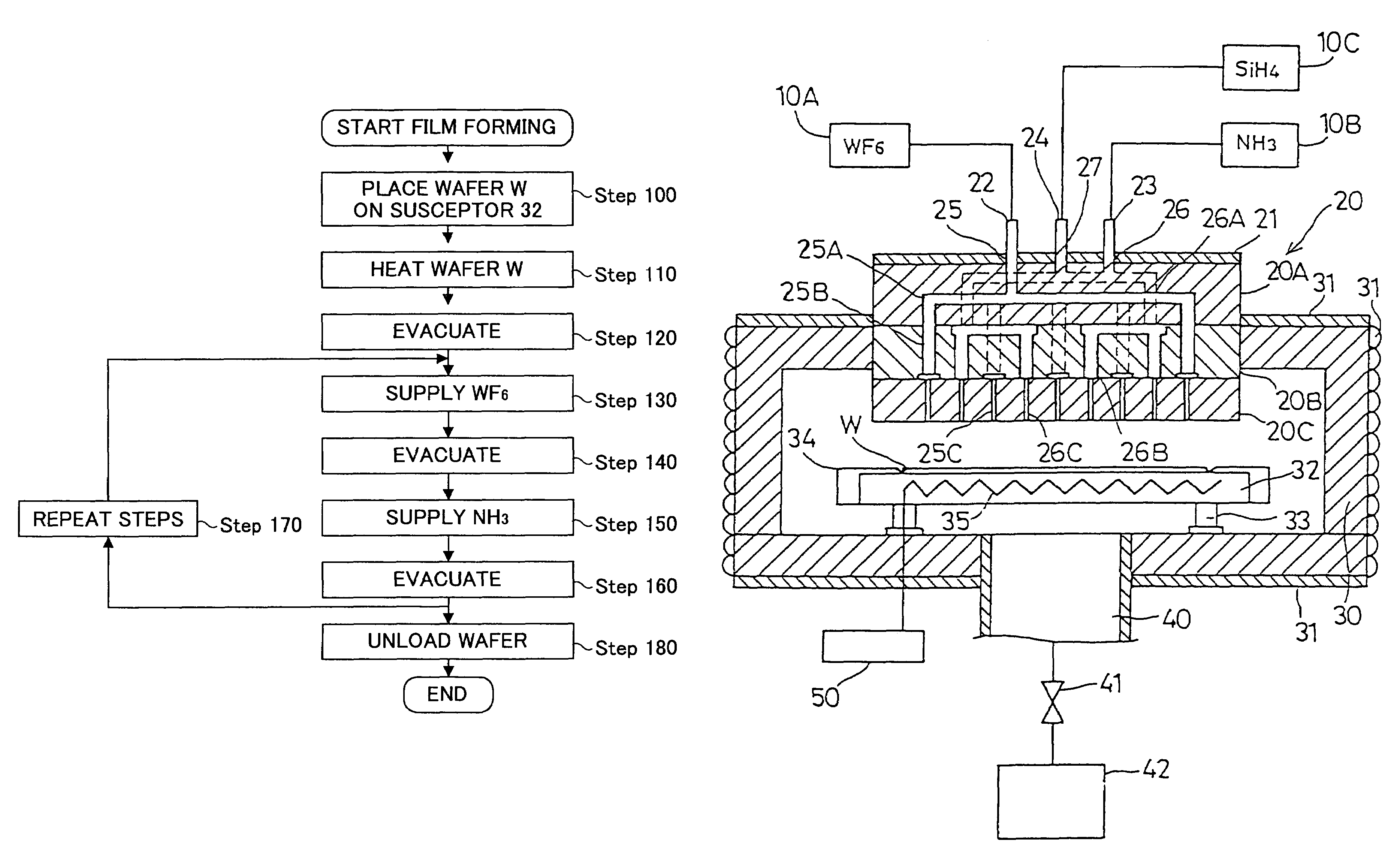
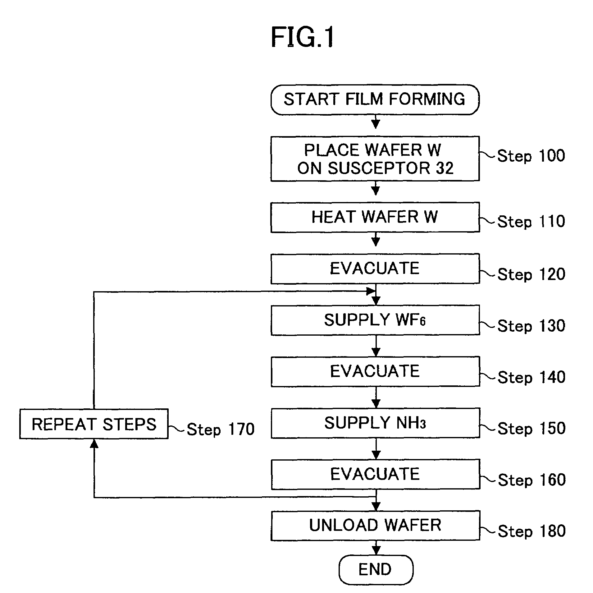
[0028]FIG. 3 shows a schematic cross-sectional view of a thin film forming apparatus (referred to as “a vacuum processing apparatus” hereinafter) for performing a thin film forming method according to one embodiment of the present invention. Prior to an explanation for a thin film forming method, an explanation will be given for the vacuum processing apparatus shown in FIG. 3, which performs the thin film forming method.

[0029]This vacuum processing apparatus includes gas supply sources 10A˜10C, a shower head 20, a shower head heater 21, a chamber 30, a heater 31, a susceptor 32, supporting members 33, an exhaust pipe 40, a valve 41, a vacuum pump 42, a power supply 50 and so on.

[0030]The gas supply sources 10A˜10C supply gasses into the chamber 30 via gas inlets 22˜24 and gas passages 25, 26, 27 provided at the shower head 20. The supplied gasses perform a predetermined fil...


PUM

PropertyMeasurementUnit
Timeaaaaaaaaaa
Thicknessaaaaaaaaaa
Temperatureaaaaaaaaaa

Abstract

The present invention relates to a method and apparatus for forming a thin film using the ALD process. Prior to the ALD process where each of a plurality of source gasses is supplied one by one, plural times, a pretreatment process is performed in which the source gasses are simultaneously supplied to shorten an incubation period and improve throughput.

Description

TECHNICAL FIELD[0001]The present invention generally relates to methods and apparatuses for forming a thin film, and more particularly, to a method and apparatus for forming a thin film by supplying each of source gasses one by one.BACKGROUND ART[0002]As semiconductor integrated circuits become more microscopic and more integrated, insulating films, metal films and other films formed on a substrate (such as a semiconductor substrate) are desired to have less thickness, better coverage for complex shapes, macroscopic uniformity over the whole wafer and microscopic smoothness at the nanometer level. However, the conventional CVD process cannot satisfy at least a portion of the above desires.[0003]At present attention is paid to the ALD (Atomic Layer Deposition) process as a film forming process that can satisfy the above desires. In the ALD process, each of different source gasses is supplied one by one, supplied source gasses are absorbed by a reactive surface and form a film at an a...

Claims


Application Information

Patent Timeline
IPC IPC(8): H01L21/44H01L21/31H01L21/469C23C16/02C23C16/34C23C16/44C23C16/455C23C16/52H01J37/32H01L21/285
CPCC23C16/0218C23C16/34C23C16/45525C23C16/45531C23C16/45565C23C16/52H01J37/32935H01L21/28556H01L21/28568C23C16/45527
Inventor YAMASAKI, HIDEAKIKAWANO, YUMIKO
Owner TOKYO ELECTRON LTD
Why Eureka
Try Eureka