Microfluidic device and method of locally concentrating electrically charged substances in a microfluidic device

a microfluidic device and local concentration technology, applied in the direction of electrostatic separators, diaphragms, electric/magnetic elements, etc., can solve the problems of long reaction time, large influence on the likelihood of interaction, and inability to achieve high-efficiency and high-efficiency. , to achieve the effect of simple and cost-effective manufacturing, increasing the reaction ra

Inactive Publication Date: 2009-02-03
STMICROELECTRONICS SRL
View PDF41 Cites 46 Cited by
  • Summary
  • Abstract
  • Description
  • Claims
  • Application Information

AI Technical Summary

Benefits of technology

[0016]In particular, the microfluidic device includes a microfluidic circuit having an axis, and an electric field generator, arranged to establish an electric field (E) within at least a section of the microfluidic circuit, the electric field (E) being oriented transversally to the axis. The electric field is used to locally concentrate charged molecules, thus increasing the reaction rate. The electric field is established using N-type and P-type semiconductor materials and is thus very simple and cost effective to manufacture.

Problems solved by technology

Some reactions, however, are lengthy and their efficiency and speed depend on several factors, such as the likelihood of interaction between the substances involved.
In particular, the likelihood of interaction is greatly affected by the concentration of the reagents.

Method used


Image

  • Microfluidic device and method of locally concentrating electrically charged substances in a microfluidic device
  • Microfluidic device and method of locally concentrating electrically charged substances in a microfluidic device
  • Microfluidic device and method of locally concentrating electrically charged substances in a microfluidic device

Examples


second embodiment

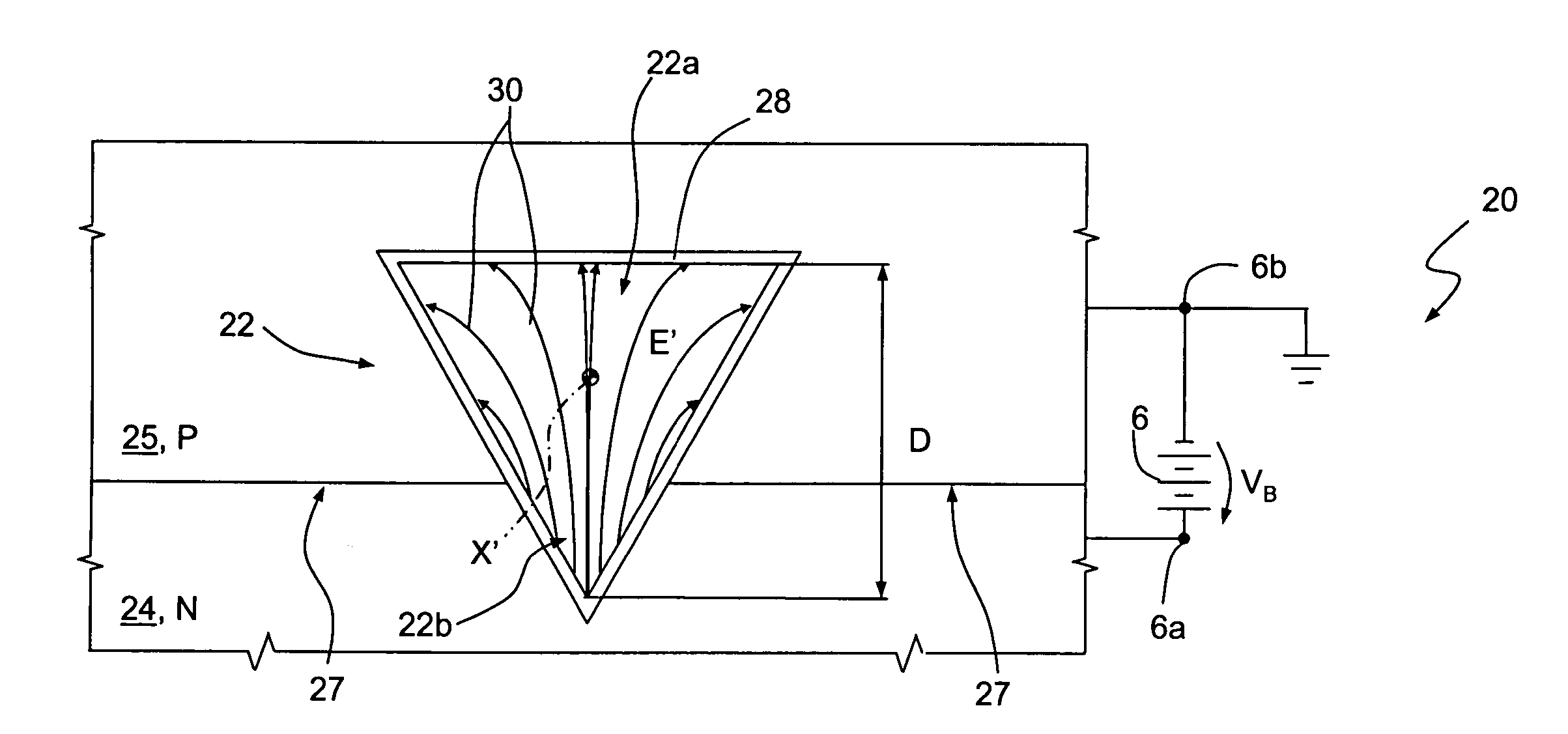
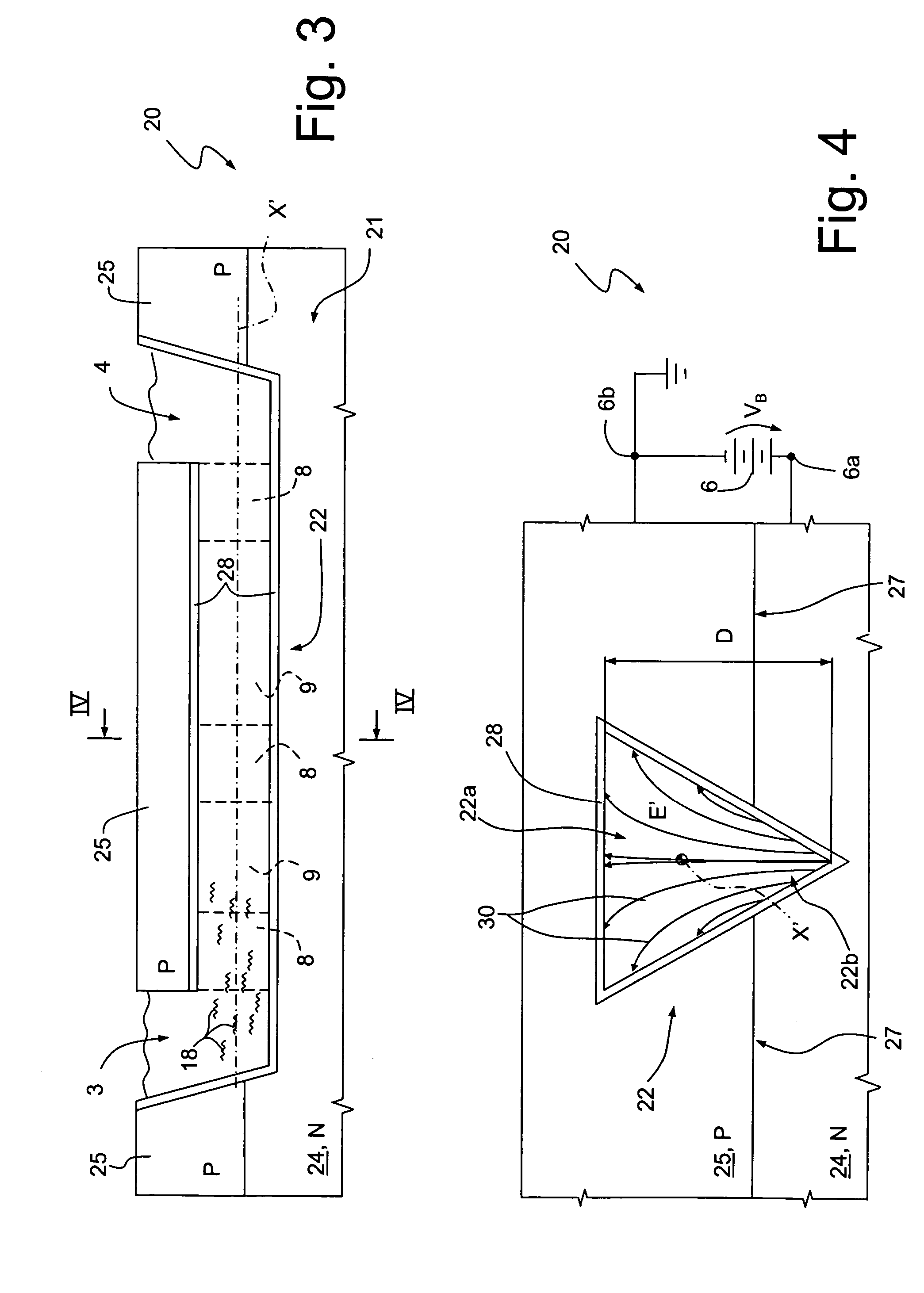
[0037] shown in FIG. 3 and 4, where parts already illustrated are indicated with the same reference numbers, a microfluidic device 21 is integrated in a semiconductor chip 20, and comprises the inlet and outlet reservoirs 3, 4, the voltage source 6 and a microfluidic circuit 22, similar to the microfluidic circuit 5 of FIGS. 1, 2. In particular, the microfluidic circuit 22 has a triangular cross section and a longitudinal axis X′, and is buried within the semiconductor chip 20. More precisely, a lower portion 22b of the microfluidic circuit 22, corresponding to approximately one third of its depth D, extends within a substrate 24 of the semiconductor chip 20, of N-type. An upper portion 22a of the microfluidic circuit 22 is both laterally and upwardly surrounded by a structural layer 25, of P-type. Moreover, the substrate 24 and the structural layer 25 are contiguous to each other and form P-N junctions 27. Also in this case, the walls of the microfluidic circuit 22 are coated with ...

third embodiment

[0041]the invention is shown in FIG. 5 and 6, where parts already illustrated are designated with the same reference numbers. In this case, a microfluidic device 41 is integrated in a semiconductor chip 40, and comprises the inlet and outlet reservoirs 3, 4, the voltage source 6 and a microfluidic circuit 42, similar to the microfluidic circuit 5 of FIGS. 1, 2. In particular, the microfluidic circuit 42 has a triangular cross section and a longitudinal axis X″, and is buried within the semiconductor chip 40. More precisely, a lower portion 42a of the microfluidic circuit 42 extends within a substrate 44 of the semiconductor chip 40, which is of N-type and is connected to the positive terminal 6a of the voltage source 6. An upper portion 42b of the microfluidic circuit 42 is both laterally and upwardly surrounded by a structural layer 45, which is of P-type and is connected to the negative terminal 6b of the voltage source 6. Moreover, the substrate 44 and the structural layer 45 are...


PUM

PropertyMeasurementUnit
thicknessaaaaaaaaaa
thicknessaaaaaaaaaa
bias voltage VBaaaaaaaaaa

Abstract

A microfluidic device includes a microfluidic circuit, having an axis, and an electric field generator, arranged to establish an electric field (E) within at least a section of the microfluidic circuit, the electric field (E) being oriented transversally to the axis. The electric field is used to locally concentrate charged molecules, thus increasing the reaction rate.

Description

PRIOR RELATED APPLICATIONS[0001]This application claims priority to application EP03425822.8, filed on Dec. 23, 2003.FEDERALLY SPONSORED RESEARCH[0002]Not applicable.SEQUENCE LISTING[0003]Not applicable.FIELD OF THE INVENTION[0004]The present invention relates to a microfluidic device, in particular a chemical microreactor for the analysis of charged molecules, such as nucleic acid, and to a method for increasing the local concentration of charged molecules in the device.BACKGROUND OF THE INVENTION[0005]As is known, microfluidic devices may be exploited in a number of applications, and are particularly suited to be used as chemical microreactors. Thanks to the design flexibility allowed by semiconductor micromachining techniques, single integrated devices have been made that are capable of carrying out individual processing steps or even an entire chemical process.[0006]In general, microfluidic chemical microreactors are provided with a microfluidic circuit, comprising a plurality o...

Claims


Application Information

Patent Timeline
Patent Type & Authority Patents(United States)
IPC IPC(8): B03C5/02B01L3/00G01N1/40
CPCB01L3/502707B01L3/502753B03C5/026B01L2200/0647B01L2300/0887B01L2400/0415G01N2001/4038
Inventor PALMIERI, MICHELE
Owner STMICROELECTRONICS SRL
Why Eureka
Try Eureka