Insulated gate silicon nanowire transistor and method of manufacture

a technology of silicon nanowires and transistors, applied in transistors, basic electric elements, nanoinformatics, etc., can solve the problems of limited development of nanosensors by modifying nanotube surfaces, only synthesizing metallic or only semiconducting nanotubes, and affecting the mechanical connection between bridging nanowires and vertical sidewalls

Inactive Publication Date: 2009-02-03
THE GOVERNMENT OF THE US SEC THE AIR FORCE
View PDF6 Cites 13 Cited by
  • Summary
  • Abstract
  • Description
  • Claims
  • Application Information

AI Technical Summary

Problems solved by technology

Although the potential of carbon nanotubes for applications such as gas-sensing field-effect devices has been demonstrated, the difficulty of synthesizing only metallic or only semiconducting nanotubes and the difficulty of modifying nanotube surfaces have limited their development as nanosensors.
However, the properties of the mechanical connection between a bridging nanowire and the vertical sidewall have not been favorable.
Although connecting electrodes to nanowires one at a time contributes to understanding the characteristics of nanowires and exploring novel device applications, it cannot be used for reproducible mass-fabrication of dense, low-cost device arrays.

Method used


Image

  • Insulated gate silicon nanowire transistor and method of manufacture
  • Insulated gate silicon nanowire transistor and method of manufacture
  • Insulated gate silicon nanowire transistor and method of manufacture

Examples


Embodiment Construction

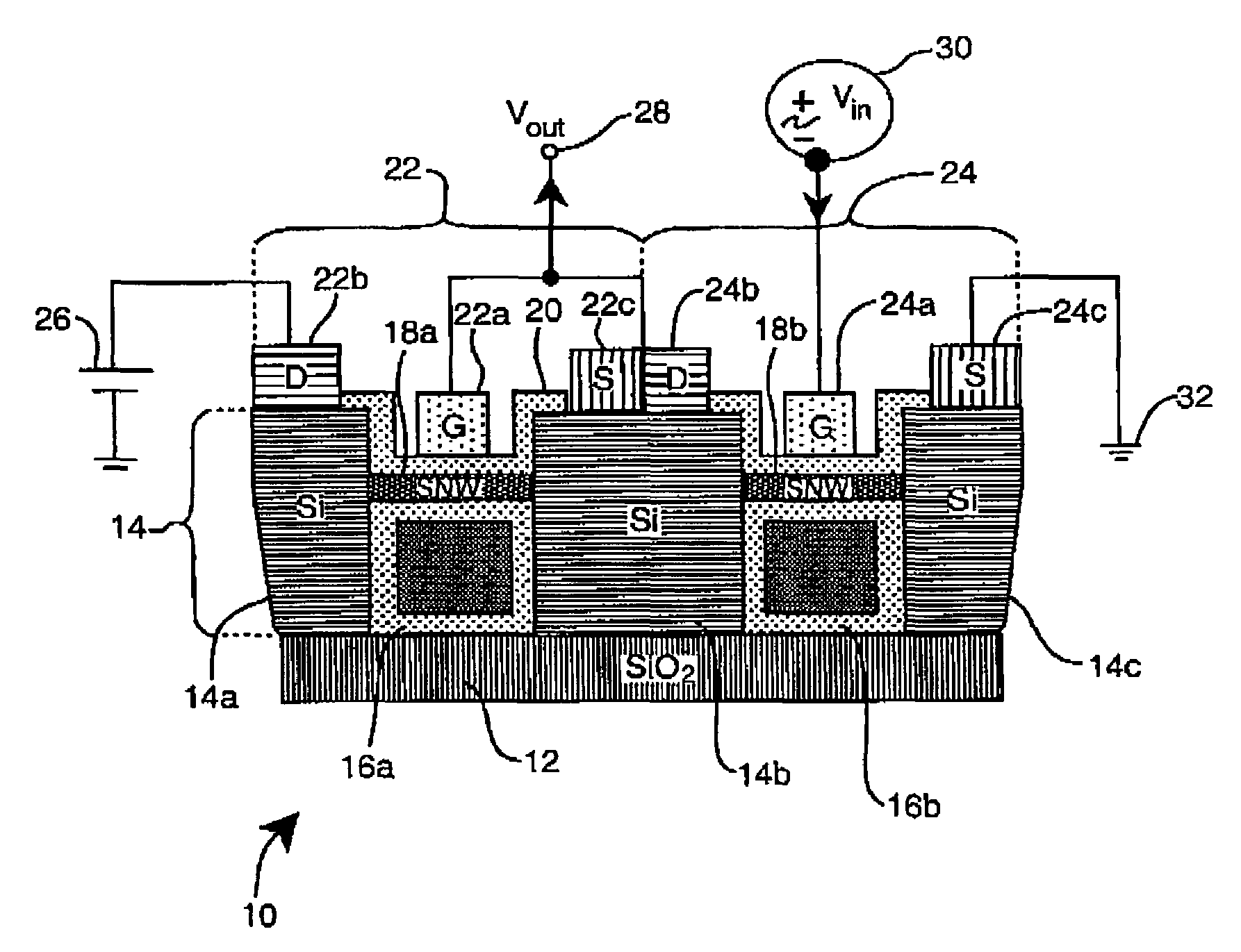
[0016]The present invention provides an insulated gate silicon nanowire transistor amplifier structure and method of manufacturing the same. The insulated gate silicon nanowire transistor amplifier structure is constructed and arranged to permit operation in the THz range by ballistically transporting electrons through a number of nanowires located within the transistor structure, as will be described in further detail below.

[0017]Referring now to FIG. 1, shown is one embodiment of the insulated gate silicon nanowire transistor amplifier structure 10 in accordance with principles of the present invention. In the illustrative embodiment, the insulated gate silicon nanowire transistor amplifier structure 10 includes a substrate 12. In an embodiment, the substrate 12 can be formed of silicon oxide, sapphire, glass or other sturdy dielectric materials or a layer of such materials deposited on a silicon substrate. A silicon layer 14 may be disposed on the substrate 12, which wafer 14 may...


PUM

PropertyMeasurementUnit
dimensionsaaaaaaaaaa
angleaaaaaaaaaa

Abstract

An insulated gate silicon nanowire transistor amplifier structure is provided and includes a substrate formed of dielectric material. A patterned silicon material may be disposed on the substrate and includes at least first, second and third electrodes uniformly spaced on the substrate by first and second trenches. A first nanowire formed in the first trench operates to electrically couple the first and second electrodes. A second nanowire formed in the second trench operates to electrically couple the second and third electrodes. First drain and first source contacts may be respectively disposed on the first and second electrodes and a first gate contact may be disposed to be capacitively coupled to the first nanowire. Similarly, second drain and second source contacts may be respectively disposed on the second and third electrodes and a second gate contact may be disposed to be capacitively coupled to the second nanowire.

Description

STATEMENT OF GOVERNMENT INTEREST[0001]The invention described herein may be manufactured and used by or for the Government for governmental purposes without the payment of any royalty thereon.FIELD OF THE INVENTION[0002]The present invention relates generally to transistor structures and, more particularly, to an insulated gate silicon nanowire transistor structure.BACKGROUND OF THE INVENTION[0003]As is known, free-standing nanostructures are currently being extensively explored. These nanostructures are especially attractive for sensor applications because their high surface-to-volume ratio makes them very sensitive to charged species adsorbed on their surfaces. Lateral growth of carbon nanotubes between two electrodes during chemical vapour deposition (CVD) has been realized for which a lateral electric field applied between the electrodes attracts the growing nanotube towards the counter-electrode. Although the potential of carbon nanotubes for applications such as gas-sensing fi...

Claims


Application Information

Patent Timeline
Patent Type & Authority Patents(United States)
IPC IPC(8): H01L27/108H01L29/76H01L29/94
CPCB82Y10/00H01L27/12H01L29/0665H01L29/0673H01L29/78696Y10S977/742Y10S977/762Y10S977/938
Inventor ANWAR, ABUL FWEBSTER, RICHARD T.
Owner THE GOVERNMENT OF THE US SEC THE AIR FORCE
Why Eureka
Try Eureka