Display device and method of manufacturing thereof

a display device and manufacturing method technology, applied in the field of display devices, can solve the problems of deteriorating low reliability of the el element, limiting the practical application of the el material, etc., and achieve the effect of enhancing the reliability of the display device, preventing moisture, and reducing the cost of production

Inactive Publication Date: 2009-02-03
SEMICON ENERGY LAB CO LTD
View PDF84 Cites 62 Cited by
  • Summary
  • Abstract
  • Description
  • Claims
  • Application Information

AI Technical Summary

Benefits of technology

[0047]According to the present invention, it is possible to prevent moisture and oxygen exist outside of a display device from penetrating into a display element in the interior of the display device via an insulating film containing an organic material with a hygroscopic property and the like. Therefore, various deteriorations caused by moisture and oxygen such as contamination of the interior of the display device, deterioration of the electric characteristics, a dark spot, and shrinkage can be prevented, thereby enhancing the reliability of the display device.
[0048]In addition, since a film constituting the display device and a film used as a protective film are simultaneously formed by a same material in the invention, the display device with high reliability can be manufactured without increasing the number of steps.
[0049]The display device manufactured above comprises a structure of blocking contaminants in a sealing region of an edge portion of a display device, and hence, the operational characteristics and reliability of the display device can be improved sufficiently. Furthermore, electronic appliances using the display device of the present invention can exhibit high degrees of reliability.

Problems solved by technology

Since the light-emitting element of the EL display device is a self-luminous type, a backlight, which is used for a conventional liquid crystal display device, is unnecessary.
However, when the EL element comprising an organic material is driven for a certain period, luminance and light emitting properties such as nonuniformity of light emission are drastically deteriorated as compared with those in the initial state, which results in a problem of low reliability.
The low reliability of the EL element is a limiting factor in practical application of the EL material.
Further, moisture and oxygen which penetrate from outside into the EL element are another factor of deteriorating the reliability of the EL element.
In an EL display device (panel) using an EL element, moisture penetrating into the interior of the device causes a serious degraded reliability, which further reads to a dark spot, shrinkage, and deterioration in luminance from a periphery of The EL display device.
Meanwhile, the shrinkage is a phenomenon in which luminance is deteriorated from edges of a pixel.
Therefore, the advantage of a thin EL display device, which dispenses with a backlight, cannot be utilized.
However, in the patent document 3, the sealing material is applied over the substrate in the sealing region as well as the patent documents 1 and 2, and therefore there is a limitation on a narrower frame formation.
The moisture and oxygen ultimately reach to the EL element via a disconnection portion in a contact hole due to poor film formation properties of source and drain electrodes and the like.
The interior of the EL display device and the EL element are contaminated by these moisture and oxygen, thereby causing various deteriorations such as deterioration of the electric characteristics, a dark spot, and shrinkage.

Method used


Image

  • Display device and method of manufacturing thereof
  • Display device and method of manufacturing thereof
  • Display device and method of manufacturing thereof

Examples


embodiment mode 1

[0073]Preferred embodiment modes of the invention will hereinafter be described with reference to the accompanying drawings.

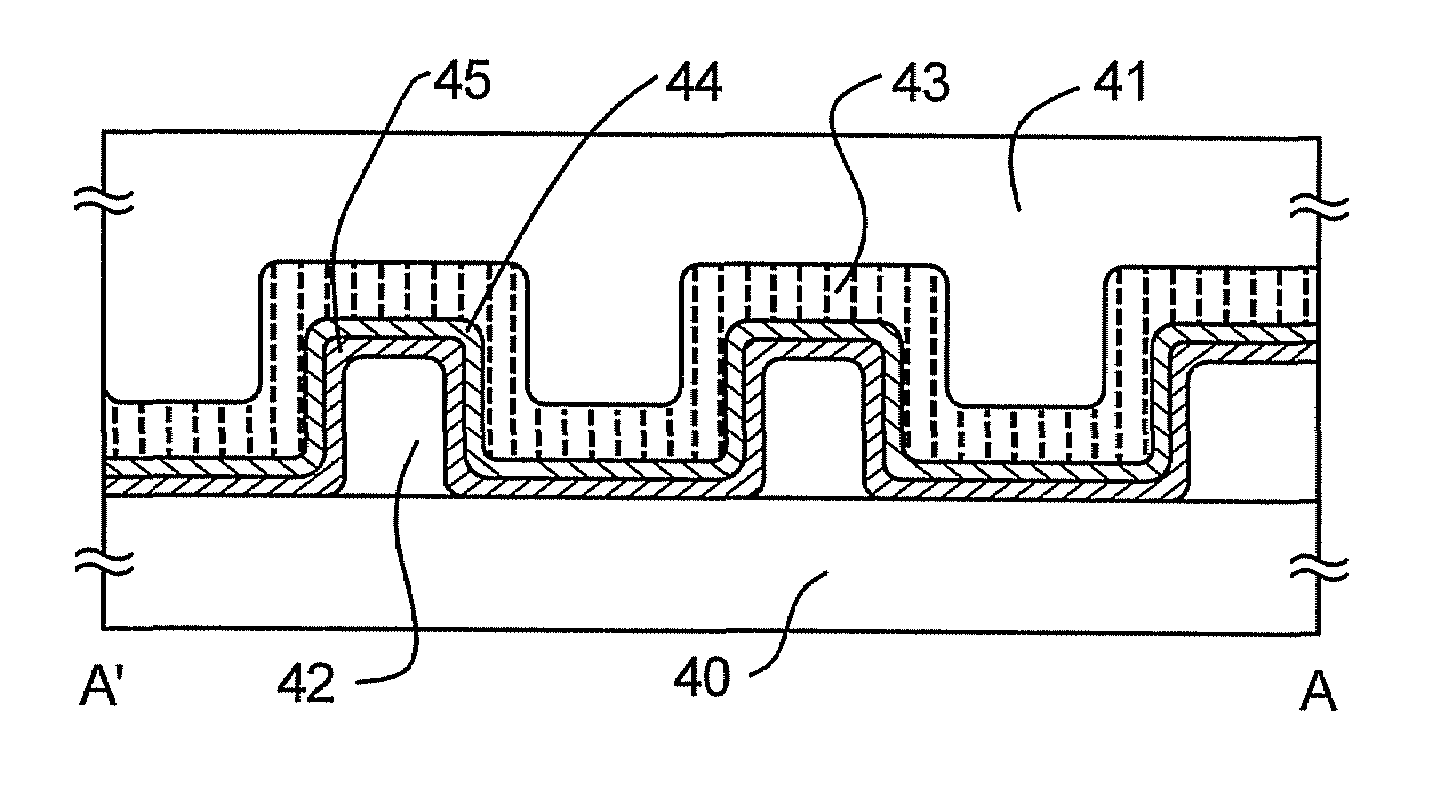
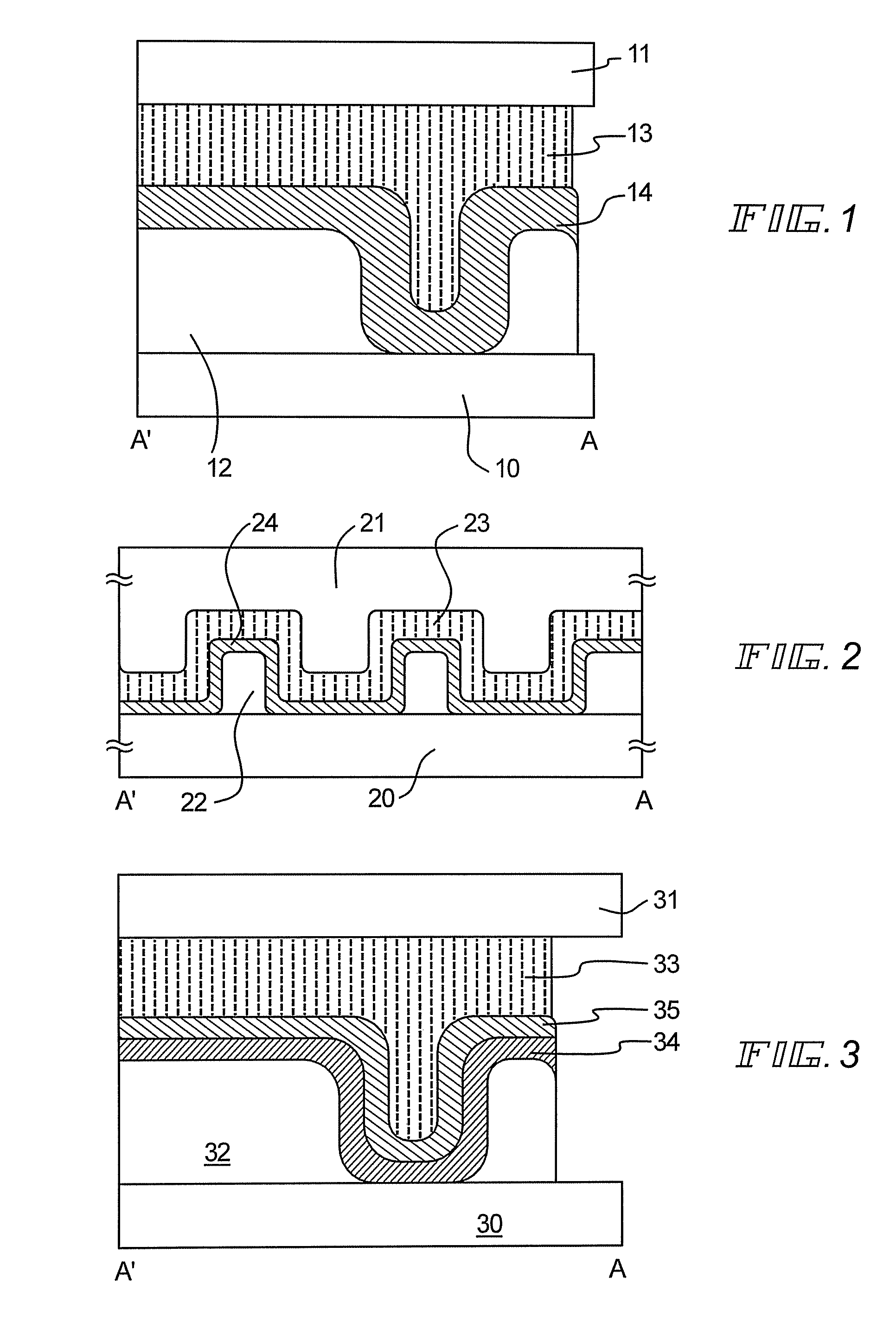
[0074]FIG. 17 is a tow view of a display device according to the present invention. An edge portion of the display device taken along a line A-A′ in FIG. 17 is described in FIG. 1. In FIG. 1, an opening is formed in an insulating layer 12 containing an organic resin material, and the opening is covered with a protective film 14. A sealing material 13 is applied over the protective film 14 so as to fill a depression due to the opening. A substrate 10 comprising the depression and opposing substrate 11 are adhered (or bonded) to each other with the sealing material 13. In the embodiment mode, the protective film 14 and wirings are made of the same material through the same steps.

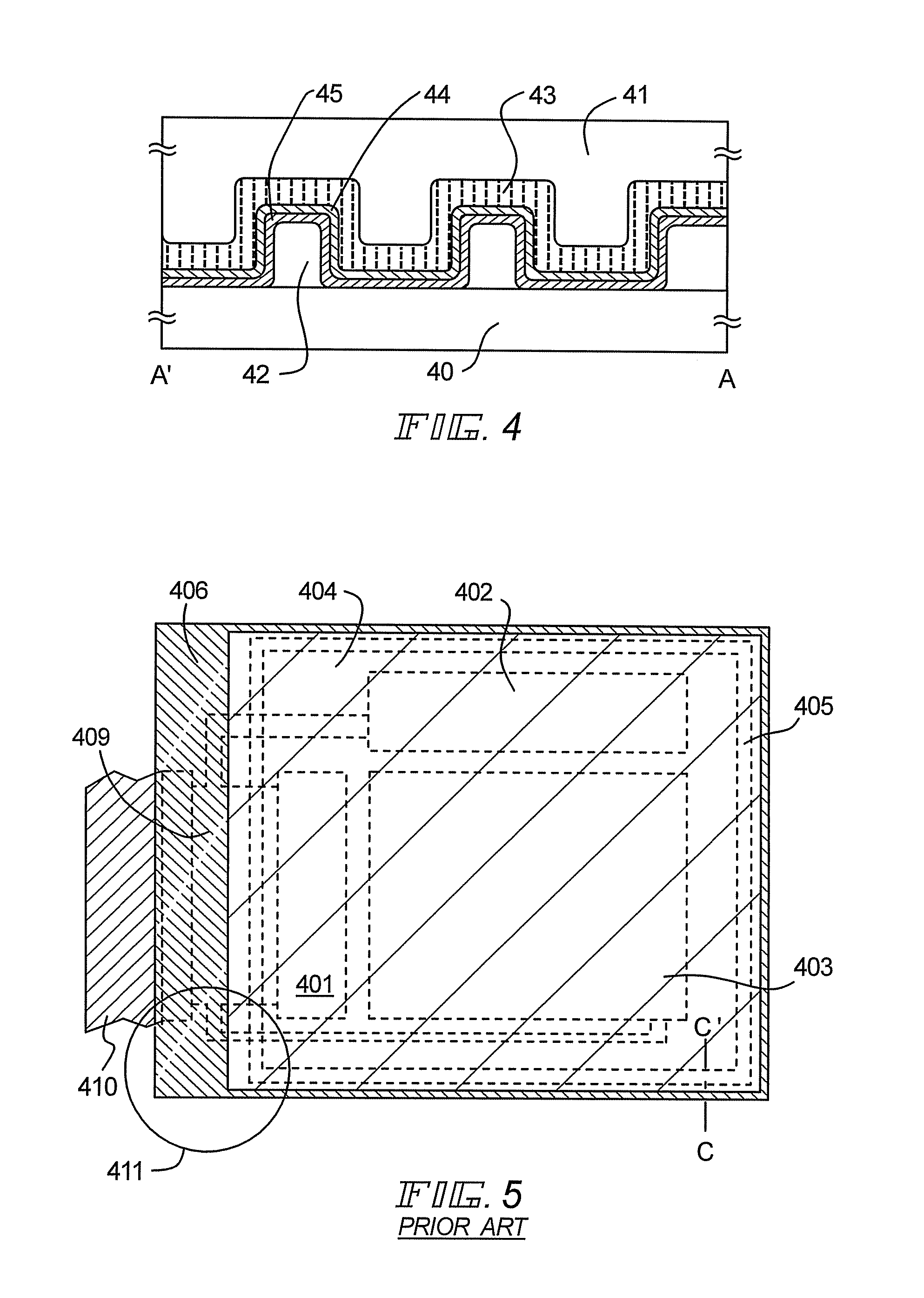
[0075]In Embodiment Mode 1, the opening is only formed in the insulating layer containing the organic resin material. However, another opening may be formed in an insulating layer on whic...

embodiment mode 2

[0084]Another embodiment mode of the present invention will hereinafter be described in more detail with reference to the accompanying drawings.

[0085]FIG. 17 is a top view of a display device according to the present invention. An edge portion of the display device taken along a line A-A′ in FIG. 17 is illustrated in FIG. 2. In FIG. 2, a plurality of openings is formed in an insulating layer 22 containing an organic resin material. The surface of the insulating layer 22 comprised depressions and projections. Each opening is covered with a protective film 24. In Embodiment Mode 2, an opposing substrate 21 attached to the substrate 20 is also comprises depressions and projections in the direction of the substrate 20 side. The opposing substrate 21 and the substrate 20 are adhered (or bonded) to each other with a sealing material 23 such that the depressions and the corresponding projections of each substrate are matched with each other.

[0086]Since the substrate 20 comprising the insul...

embodiment

Embodiment 1

[0099]In Embodiment 1, an example of manufacturing a display device having a dual emission structure according to the present invention will hereinafter be described. In the present invention, a display panel in which an EL element formed on a substrate is sealed between the substrate and a covering material and a display module comprising TFTs in the display panel are generically referred to as the display device. The EL element comprises a layer including an organic compound that generates electroluminescence (a light emitting layer), an anode layer, and a cathode layer. Luminescence obtained from organic compounds is classified into light emission upon returning to the base state from singlet excited state (fluorescence) and light emission upon returning to the base state from triplet excited state (phosphorescence). EL materials, which can be used for the present invention, include all light-emitting materials that emit photons via either the singlet excited state or...


PUM

PropertyMeasurementUnit
thicknessaaaaaaaaaa
thicknessaaaaaaaaaa
thicknessaaaaaaaaaa

Abstract

A novel display device with higher reliability having a structure of blocking moisture and oxygen, which deteriorate the characteristics of the display device, from penetrating through a sealing region and a method of manufacturing thereof is provided. According to the present invention, a display device and a method of manufacturing the same comprising: a display portion formed by aligning a light-emitting element using an organic light-emitting material between a pair of substrate, wherein the display portion is formed on an insulating layer formed on any one of the substrates, the pair of substrates is bonded to each other with a sealing material formed over the insulating layer while surrounding a periphery of the display portion, at least one layer of the insulating layer is made of an organic resin material, the periphery has a first region and a second region, the insulating layer in the first region has an opening covered with a protective film, the sealing material is formed in contact with the opening and the protective film, an outer edge portion of the insulating layer in the second region is covered with the protective film or the sealing material.

Description

BACKGROUND OF THE INVENTION[0001]1. Field of the Invention[0002]The present invention relates to a display device comprising an element (hereinafter referred to as a light-emitting element) in which a light-emitting material is interposed between a pair of electrode, and to a method of manufacturing thereof. More particularly, the present invention relates to a sealing structure of a display device using a light-emitting material that generates electroluminescence (EL) and a method of manufacturing the same.[0003]2. Description of the Related Art[0004]In recent years, development of a display device (EL display device) using a light-emitting element (hereinafter referred to as an EL element) which utilizes electroluminescent phenomenon of a light-emitting material has been advanced. Since the light-emitting element of the EL display device is a self-luminous type, a backlight, which is used for a conventional liquid crystal display device, is unnecessary. In addition, the EL display...

Claims


Application Information

Patent Timeline
Patent Type & Authority Patents(United States)
IPC IPC(8): G02F1/1339G02F1/136G02F1/1333H05B33/04H05B33/10H05B33/12H05B33/14H05B33/22
CPCH01L51/5237H01L33/44H05B33/14H05B33/04H01L2251/5323Y10T428/24777H10K59/122H10K2102/3031H10K59/8722H10K50/8426H10K50/84H10K59/124H10K59/131H10K59/1213H10K59/1201H01L23/564H01L27/124
Inventor SAKAKURA, MASAYUKIGODO, HIROMICHITSUCHIYA, KAORU
Owner SEMICON ENERGY LAB CO LTD
Why Eureka
Try Eureka