

Radiation detector and method for producing photoconductive layer for recording thereof
a technology of photoconductive layer and radioactive layer, which is applied in the direction of conversion screen, instruments, nuclear engineering, etc., can solve the problems of low sensitivity of the layer, many structural defects in the photoconductive layer made of amorphous selenium, etc., and achieve high electron transportability and greatly improved hole transportability
- Summary
- Abstract
- Description
- Claims
- Application Information
AI Technical Summary
Benefits of technology
Problems solved by technology
Method used
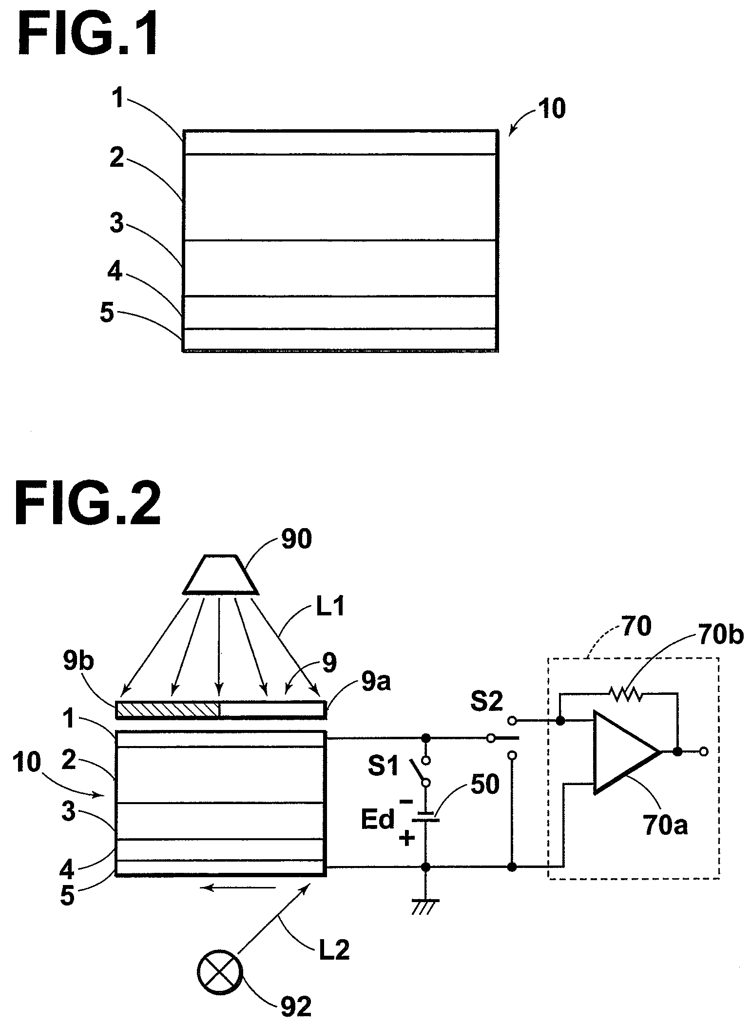
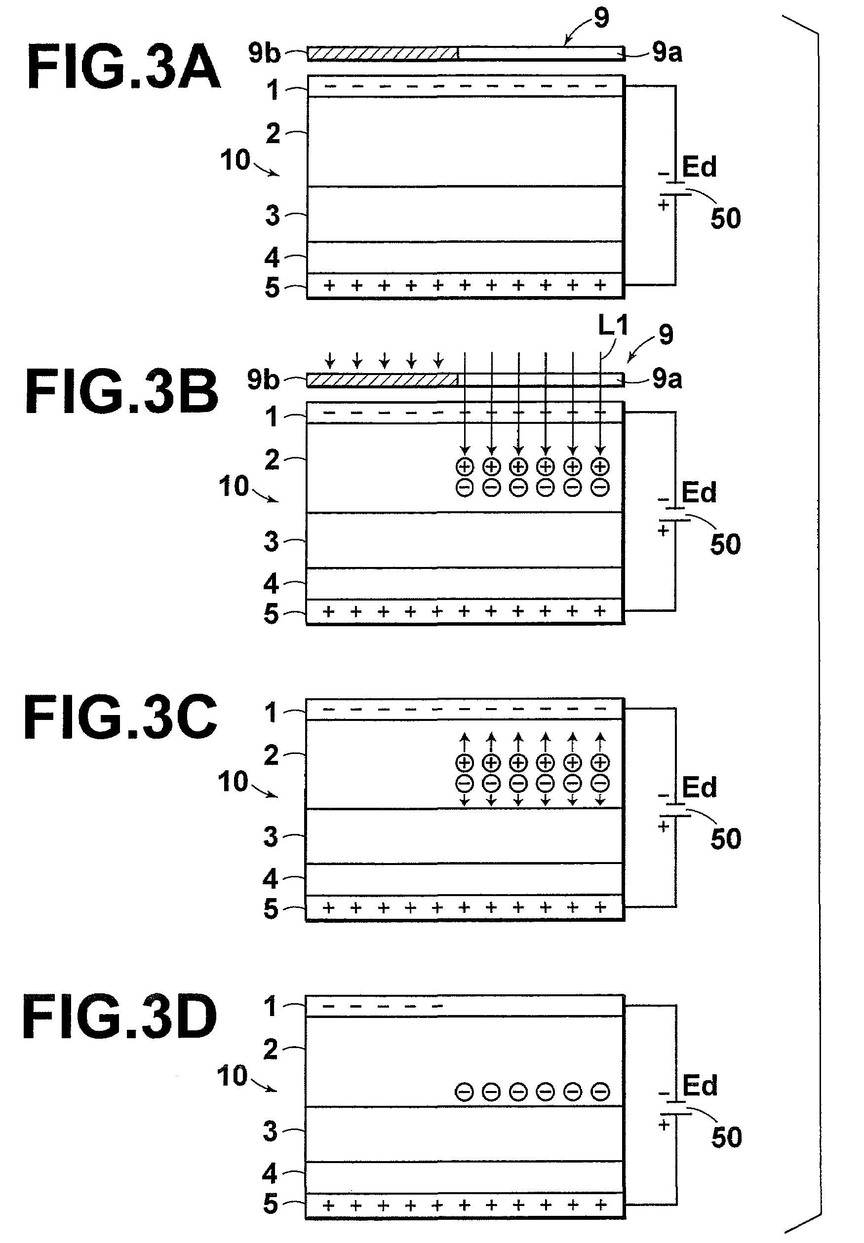
Image

Examples
examples
Samples 1 through 4
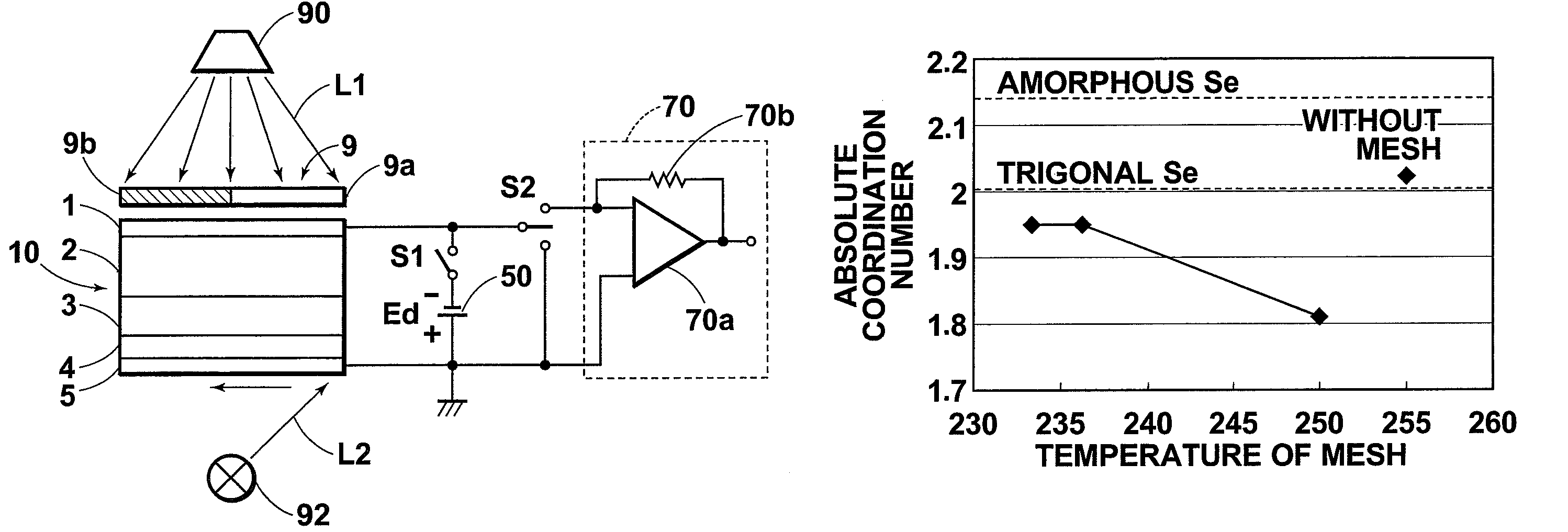
[0088]Selenium containing sodium at approximately 10 ppm was heated in a vapor-deposition cell to which a metal mesh (#300 (mesh count per inch of the mesh is 300)) made of stainless steel was attached. The temperature of the mesh was controlled in the range of the melting point (220) of selenium to 250° C. , as shown in Table 1, and selenium was deposited at 100 to 200 μm by evaporation. The temperature of the mesh was measured at the frame of the mesh.
Sample 5
[0089]Selenium containing sodium at approximately 10 ppm was heated at a vapor-deposition source temperature of 255° C. , and selenium was deposited at 100 to 200 μm by evaporation.
[0090]The selenium layer (film or coating) of each of samples 1 through 5 was measured to obtain a coordination number, distribution of the densities of states of holes at a localized level (DOS [×1013 eV−1·cm−3]) and value μτ of holes (hole range (distance) per unit electric field×10−6 cm2 / V) of the layer.
[0091]The coordination ...
PUM
| Property | Measurement | Unit |
|---|---|---|
| melting point | aaaaa | aaaaa |
| size | aaaaa | aaaaa |
| thickness | aaaaa | aaaaa |
Abstract
Description
Claims
Application Information