Semiconductor integrated circuit

a technology of integrated circuits and semiconductors, applied in the direction of semiconductor devices, semiconductor/solid-state device details, instruments, etc., can solve the problems of stress caused, warpage, and malfunction of the integrated circuit of the semiconductor,

Inactive Publication Date: 2009-03-03
SHARP KK
View PDF10 Cites 8 Cited by
  • Summary
  • Abstract
  • Description
  • Claims
  • Application Information

AI Technical Summary

Benefits of technology

[0017]According to each of the above semiconductor integrated circuits of the present invention, because a shielding film covers the entire surface of a chip at a certain shielding rate, even if unsealing the resin covering a semiconductor integrated circuit and exposing it to the surface of a semiconductor substrate, visual observation of a circuit device or circuit wiring from the outside of a chip or circuit analysis by a probe such as an electronic beam becomes very difficult. Particularly, by decreasing the width of an opening, physical probing or electromagnetically probing by an electronic beam becomes very difficult or impossible. It is preferable that the width of the opening is approx. 10 μm or less. In this case, it is allowed that the length of the opening is larger than the width of it. As a result, it is possible to effectively prevent the information in a semiconductor integrated circuit from being taken out for an illegal purpose.
[0034]Furthermore, when a treatment for increasing a crystal defect density is applied to the back of a semiconductor substrate, the defect density on the back of the semiconductor substrate becomes larger than the crystal defect density of a normal non-defective wafer. Therefore, the infrared radiation incoming from the back of the semiconductor substrate is irregularly reflected by crystal defects in the semiconductor substrate and it is possible to prevent observation from the back of a circuit device on the surface of the semiconductor substrate.

Problems solved by technology

Moreover, there is a problem that electromagnetic noises are radiated to the outside of a semiconductor integrated circuit to cause another semiconductor integrated circuit to malfunction depending on the amplitude of a clock signal or the like in the semiconductor integrated circuit and a hazard that the semiconductor integrated circuit malfunctions due to electromagnetic noises from another unit.
However, as described above, by forming the shielding film 1 on almost the entire surface of the semiconductor chip, a problem occurs that a stress caused by a difference between thermal expansion coefficients of the shielding film 1 and an interlayer insulating film 7 or a difference between thermal expansion coefficients of the shielding film 1 and a semiconductor substrate 4 increases and a shift between the shielding film 1 and interlayer insulating film 7 increases or a warpage increases when the semiconductor chip is thin.
However, because the aluminum film covers almost the entire surface, thermal expansion cannot be absorbed, a convex warpage occurs which is formed when the central portion of a wafer protrudes, a shift occurs between the shielding film and interlayer insulating film, and resultantly a device malfunctions.
Furthermore, when forming a plane not parallel with the surface of a semiconductor substrate on the back of the substrate as a countermeasure to prevent analysis by applying infrared radiation from the backside of the semiconductor substrate, a warpage occurs in which the central portion of the surface of the semiconductor substrate becomes convex.
Therefore, it is difficult to use the shielding film for the entire surface.

Method used


Image

  • Semiconductor integrated circuit
  • Semiconductor integrated circuit
  • Semiconductor integrated circuit

Examples


second embodiment

(Second Embodiment)

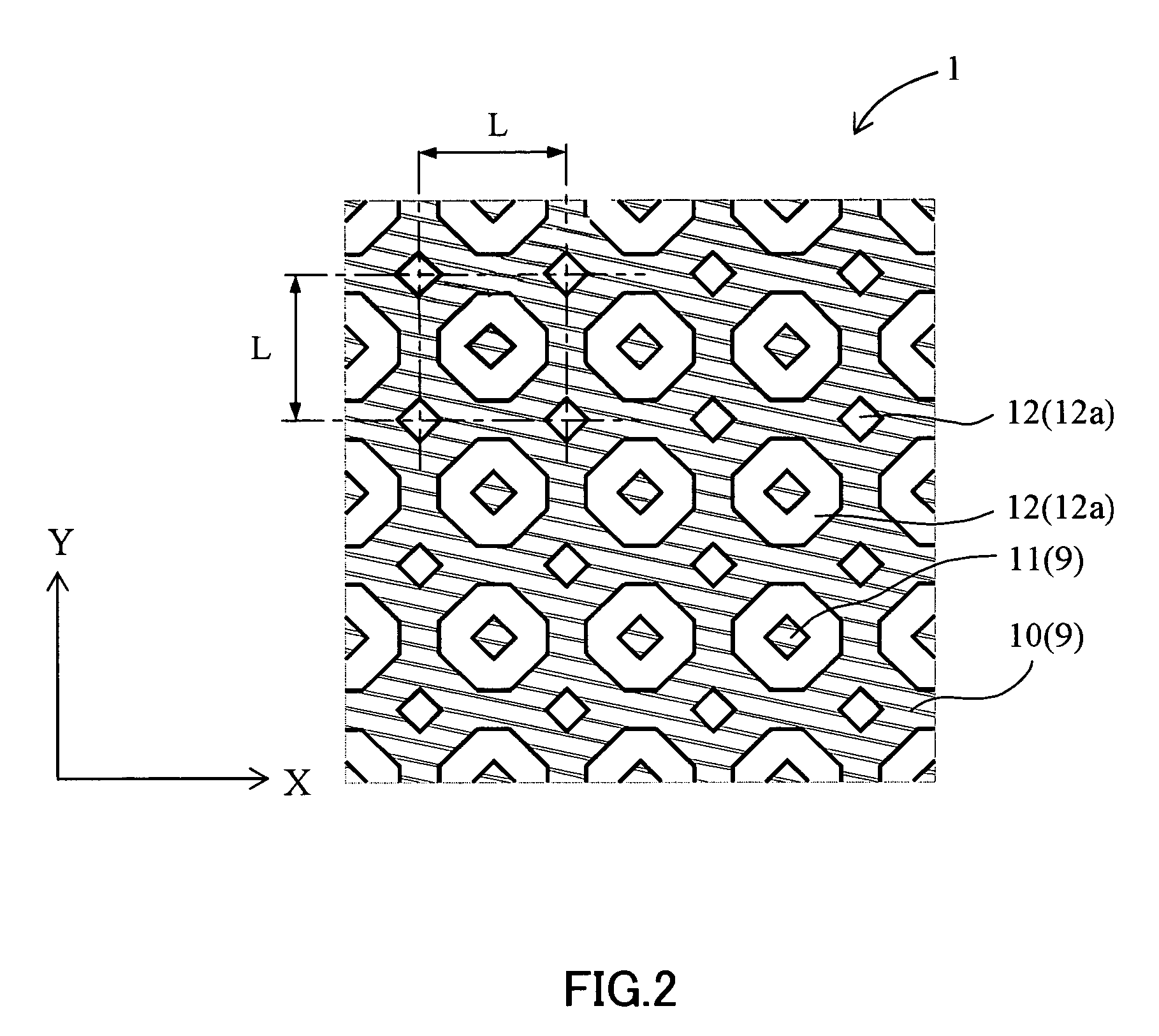
[0064]FIG. 5 shows a pattern (portion) and a top viewed structure of the shielding film 1 of the present invention circuit 100 of the second embodiment. The sectional structure of the present invention circuit 100 is the same as the first embodiment. The difference from the first embodiment is the pattern shape of the shielding film 1. In the case of the shielding film pattern of the first embodiment, the opening 12 and independent shielding portion 11 are formed in one large continuous shielding portion 10. In the case of the second embodiment, however, the continuous shielding portion 10 is divided into two continuous shielding portions 10a and 10b by an isolating space 35. Thus, when a plurality of continuous shielding portions 10 are present by being electrically isolated, it is possible to use the continuous shielding portions 10a and 10b as power supply wirings having potential levels different from each other. In this case, by connecting the continuous shie...

third embodiment

(Third Embodiment)

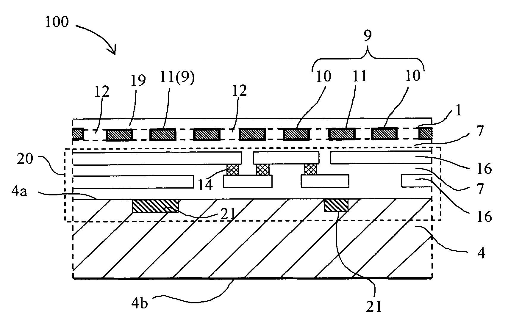
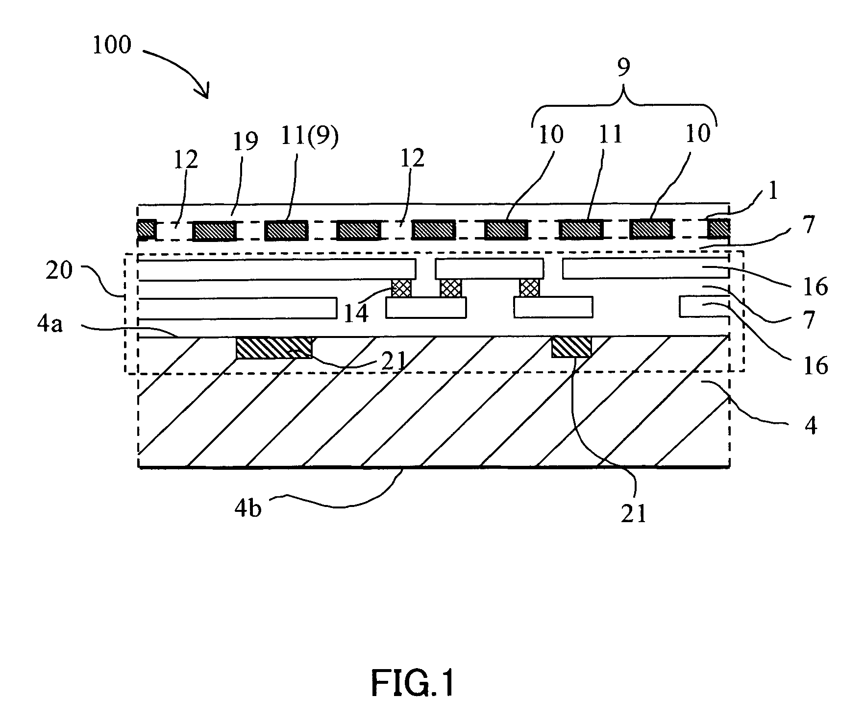
[0067]FIG. 10 schematically shows a sectional structure of a present invention circuit 101 of third embodiment. The present invention circuit 101 is different from the present invention circuit 100 in that shielding films 1 are constituted by two layers and have a upper shielding film 1a and a lower shielding film 1b. How to form a circuit device portion 21, signal wiring, shielding films 1a and 1b, and interlayer insulating film 7 and a material used and film thickness are the same as the case of the first embodiment. However, the lower shielding film 1b has the same thickness as the metallic wiring 16.

[0068]In the case of the third embodiment, it is possible to completely shield a circuit structure portion 20 by using two layers of the shielding film 1 of the upper shielding film 1a and the lower shielding film 1b and prevent the circuit structure portion 20 from optical observation by an optical microscope or observation by an electronic beam tester. Each of two...

fourth embodiment

(Fourth Embodiment)

[0072]FIG. 13 schematically shows a sectional structure of a present invention circuit 102 of fourth embodiment. The present invention circuit 102 of the fourth embodiment is different from the present invention circuit 101 of the third embodiment in that shielding portions of the upper shielding film 1a and a lower shielding film 1b are used as power supply wirings. Continuous shielding portions 10 of the upper shielding film 1a and the lower shielding film 1b are electrically connected with the metallic wiring 16 of a circuit structure portion 20 through a connection layer 14. To connect the continuous shielding portion 10 of the upper shielding film 1a to the metallic wiring 16, the portion 10 is temporarily electrically connected with the independent shielding portion 11 of the lower shielding film 1b through the connection layer 14 and the independent shielding portion 11 of the lower shielding film 1b is connected to the metallic wiring 16 through the connec...


PUM


Abstract

In a semiconductor integrated circuit (100) having a shielding film (1) formed by a material different from at least either of a semiconductor substrate (4) and an interlayer insulating film (7) in thermal expansion coefficient, the shielding film (1) has shielding portions (9) and openings (12), and at least either of a plurality of independent openings (12a) whose circumferences are surrounded by the shielding portions (9) and a plurality of independent shielding portions (11) whose circumferences are surrounded by the openings (12) is present and scattered on the entire surface of a chip. Or, a plurality of openings (12) are present on an optional straight line parallel with the surface (4a) of the semiconductor substrate (4) passing through a portion for shielding circuit devices (21) and circuit wirings (16) in the shielding portions (9).

Description

[0001]This Nonprovisional application claims priority under 35 U.S.C. § 119(a) on Patent Application No(s). 2003-295958 filed in Japan on Aug. 20, 2003, the entire contents of which are hereby incorporated by reference.BACKGROUND OF THE INVENTION[0002]1. Field of the Invention[0003]The present invention relates to a semiconductor integrated circuit, particularly to an art effectively applied to a semiconductor integrated circuit having a multilayer wiring structure.[0004]2. Description of the Related Art[0005]In the case of a semiconductor integrated circuit, a product is born which has a multilayer wiring structure constituted by forming a large-scale circuit device group on the surface of a semiconductor substrate and alternately heaping an insulating layer and a wiring layer to be electrically connected. Some of the semiconductor integrated circuits have a memory in which important confidential information is included or a circuit including an advanced intellectual property. Ther...

Claims


Application Information

Patent Timeline
Patent Type & Authority Patents(United States)
IPC IPC(8): H01L23/552G06K19/077H01L21/3205H01L21/822H01L23/52H01L23/522H01L23/58H01L27/04
CPCH01L23/5225H01L23/552H01L23/57H01L2224/16145H01L2924/13091H01L21/3205
Inventor HENMI, TAKUYA
Owner SHARP KK
Why Eureka
Try Eureka