Sense amplifier circuit in semiconductor memory device and driving method thereof

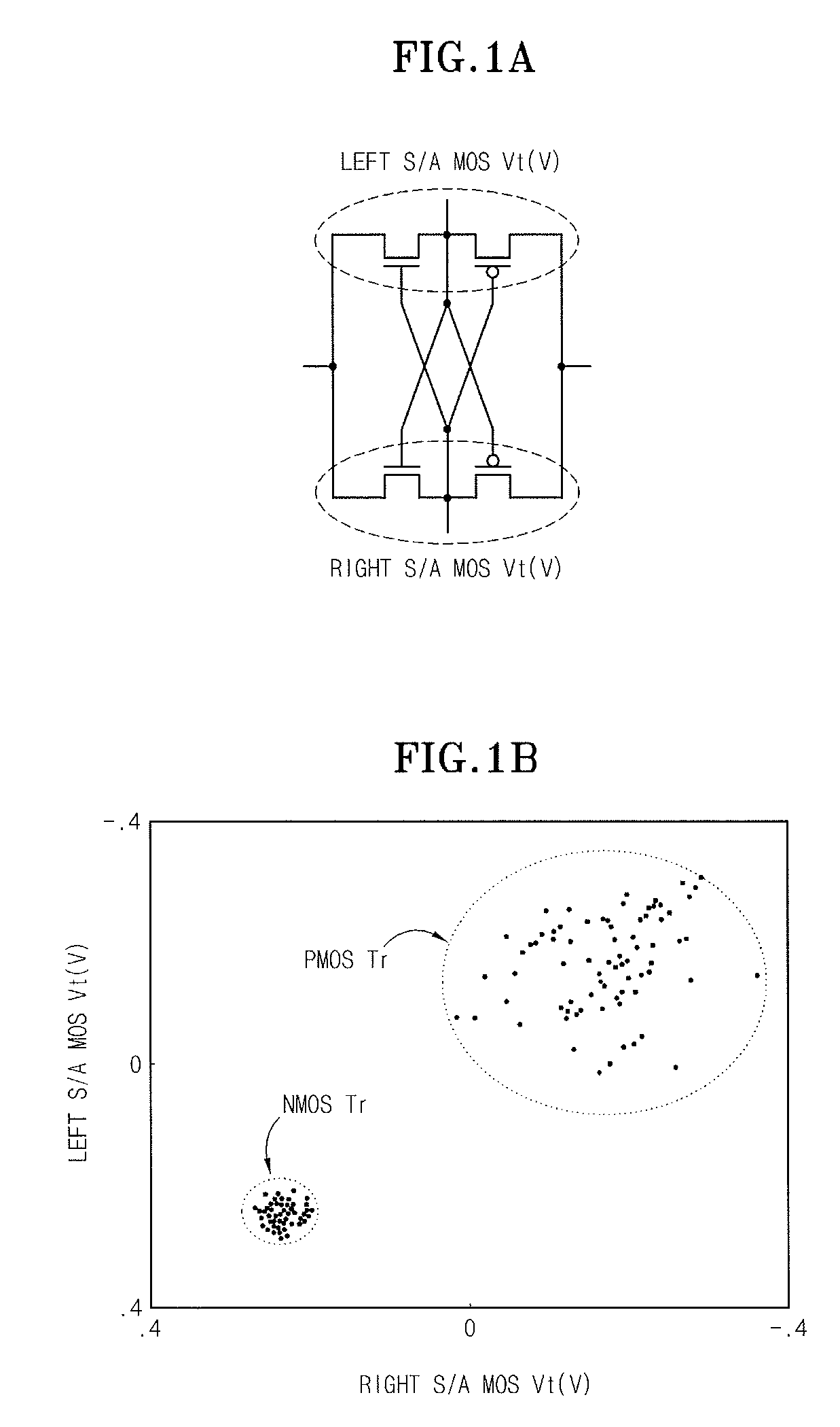
a technology of memory device and amplifier circuit, which is applied in the direction of digital storage, instruments, balustrades, etc., can solve the problems of deteriorating operation feature of sensor amplifier, insufficient operation voltage margin of threshold voltage of nmos transistor or pmos transistor, and deteriorating driving capability of amplifier, so as to improve the driving capability of sense amplifier

Inactive Publication Date: 2009-03-17
SK HYNIX INC
View PDF4 Cites 22 Cited by
  • Summary
  • Abstract
  • Description
  • Claims
  • Application Information

AI Technical Summary

Benefits of technology

[0024]In order to solve the aforementioned problems, the present invention improves driving capability of a sense amplifier by performing an under-drive at a drive time point.
[0025]The present invention also prevents erroneous data that is produced by an over-drive from being output from the sense amplifier by concurrently performing the under-drive and the over-drive.
[0026]The present invention also increases a speed when data is read from or written in a cell by enhancing driving capability of the sense amplifier.

Problems solved by technology

In general, as a low voltage is gradually applied for an operation of a semiconductor memory device, an operation voltage margin for a threshold voltage of an NMOS transistor or a PMOS transistor becomes insufficient.
As a result, an operation feature of a sensor amplifier deteriorates.
In the case of a low voltage operation, driving capability of an amplifier deteriorates.
On the other hand, in the case of PMOS transistors, the threshold voltage features the left PMOS transistor and the right PMOS transistor are dispersed, thereby showing non-uniform distribution.
Regarding the operation voltage of the semiconductor memory device operated in the aforementioned manner, as described above, the operation voltage margin for the threshold voltages of the NMOS transistor and the PMOS transistor included in the sense amplifier becomes insufficient.
As a result, the operation feature of the sense amplified deteriorates.
Therefore, in the case of a low voltage operation, amplification driving capability of the sense amplifier decreases.
However, since a PMOS offset feature has a significant effect on the over-drive method, erroneous data may be output from the sense amplifier.

Method used


Image

  • Sense amplifier circuit in semiconductor memory device and driving method thereof
  • Sense amplifier circuit in semiconductor memory device and driving method thereof
  • Sense amplifier circuit in semiconductor memory device and driving method thereof

Examples


Embodiment Construction

[0048]Hereinafter, exemplary embodiments of the present invention will be described in detail with reference to the accompanying drawings.

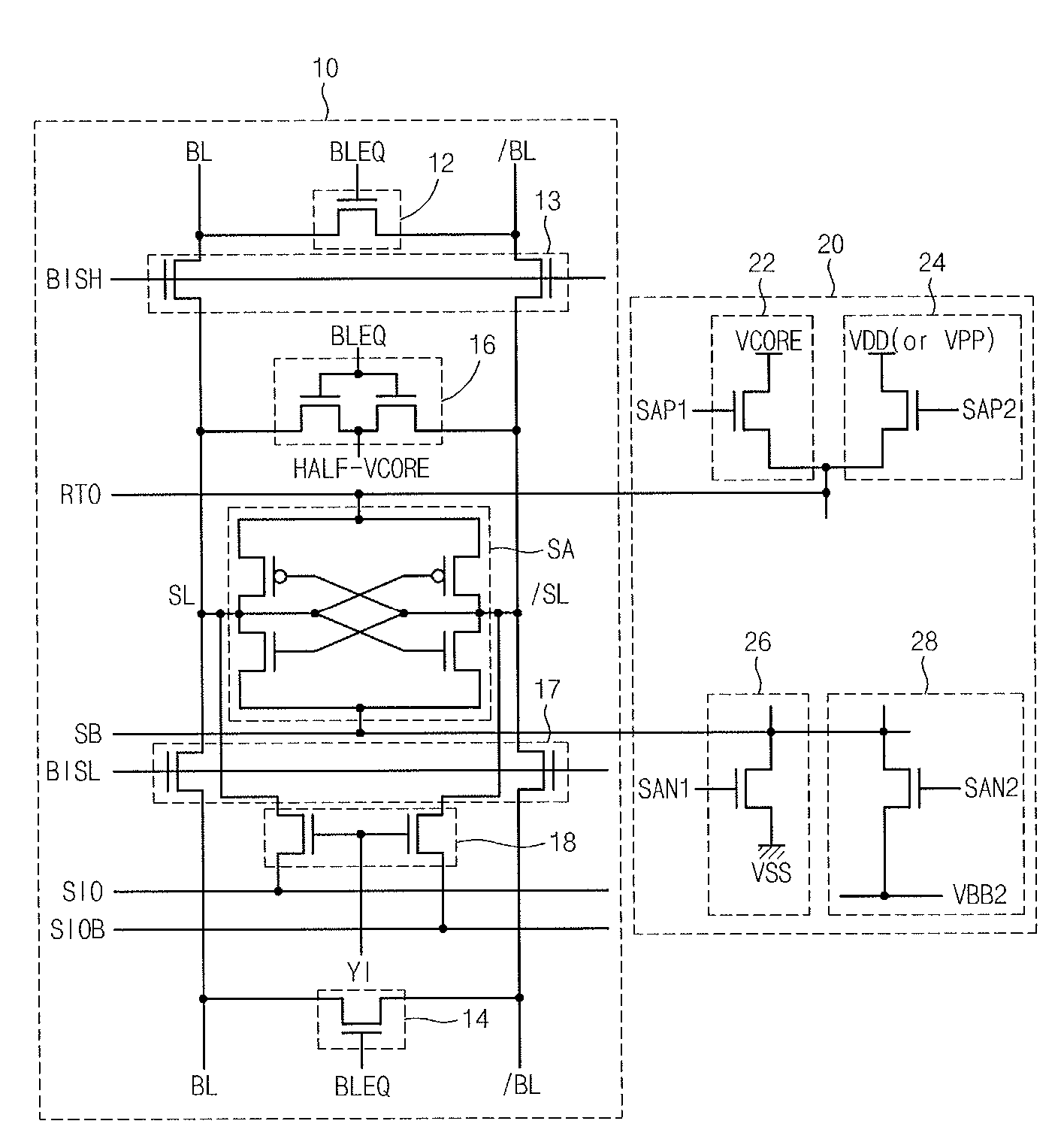
[0049]FIG. 5 is a circuit diagram of a folded bit line structure employed by a sense amplifier circuit in a semiconductor memory device according to an embodiment of the present invention. A sense amplifier 10 is formed between bit lines BL and / BL. A drive controller 20 is formed to supply a pull-up voltage and a pull-down voltage to a sense amplifier SA of the sense amplifier 10.

[0050]A pair of equalizers 12 and 14, a pre-charger 16, and the sense amplifier SA are formed in parallel between the bit lines BL and / BL. The pre-charger 16 and the sense amplifier SA are formed between the pair of equalizers 12 and 14. A bit line selector 13 is formed over the bit lines BL and / BL between the equalizer 12 and the pre-charger 16. Another bit line selector 17 is formed over the bit line BL and / BL between the equalizer 14 and the sense amplifier SA.

[005...


PUM


Abstract

Provided is a sense amplifier circuit in a semiconductor memory device in which an under-drive is applied to a switching element of a pull-down side of a sense amplifier in order to compensate for poor driving capability in the case of performing a low voltage operation. The sense amplifier circuit includes: a sense amplifier which has a pull-down element composed of an NMOS transistor and a pull-up element composed of a PMOS transistor and is formed between bit lines to perform data exchange; and a drive controller which supplies a drive voltage for the use of pull-up and pull-down operations to the sense amplifier in order to perform the data exchange, and, during a specific time period included in a time for providing the drive voltage, performs an under-drive whereby the drive voltage for the use of the pull-down operation is used so that the sense amplifier is provided with a voltage that is lower than a voltage used in the pull-down operation in a normal state.

Description

TECHNICAL FIELD[0001]The present invention relates to a sense amplifier circuit in a semiconductor memory device, and more particularly, to a sense amplifier circuit in a semiconductor memory device in which an under-drive is applied to a switching element of a pull-down side of a sense amplifier in order to compensate for poor driving capability in the case of performing a low voltage operation.BACKGROUND ART[0002]In general, as a low voltage is gradually applied for an operation of a semiconductor memory device, an operation voltage margin for a threshold voltage of an NMOS transistor or a PMOS transistor becomes insufficient. As a result, an operation feature of a sensor amplifier deteriorates.[0003]The sense amplifier includes an NMOS transistor for a pull-down operation and a PMOS transistor for a pull-up operation. There are significant changes in an average value of threshold values of the NMOS transistor and the PMOS transistor constituting the sense amplifier. The different...

Claims


Application Information

Patent Timeline
Patent Type & Authority Patents(United States)
IPC IPC(8): G11C7/00
CPCG11C7/065G11C7/08G11C11/4074G11C11/4091G11C2207/065G11C2207/2227E04F11/1836A01G9/045E04F2011/1872E04F2011/188
Inventor KANG, HEE BOK
Owner SK HYNIX INC
Why Eureka
Try Eureka