Semiconductor laser device and manufacturing method thereof

a laser device and semiconductor technology, applied in the field of semiconductor laser devices, can solve the problems of increasing the resistivity of the entire infrared laser element, the difficulty of forming window structures for both laser elements at the same time, and the disadvantage of high power output, so as to reduce the number of manufacturing steps, improve the reliability of the device, and reduce the effect of manufacturing steps

Inactive Publication Date: 2009-03-17
PANASONIC CORP
View PDF13 Cites 6 Cited by
  • Summary
  • Abstract
  • Description
  • Claims
  • Application Information

AI Technical Summary

Benefits of technology

[0023]It addition, in manufacturing a monolithic dual-wavelength laser device, the same material is used for cladding layers of both the red and infrared laser elements to reduce the number of manufacturing steps. Normally, the cladding layers are made of an AlGaInP material. In this case, the compositions of the respective cladding layers may be adjusted for optimum performance. As a result, the cladding layers of the red and infrared laser elements mutually differ in the Zn diffusion coefficients. The difference can not be accommodated only by chaining the thickness of the active layers.
[0024]The present invention relates to a manufacturing method of a monolithic dual-wavelength semiconductor laser device with a simple structure, and aims to allow the active layers of infrared and red laser elements to be disordered by thermally diffusing Zn all at once, while ensuring high reliability of the device.
[0026]With the above semiconductor laser device according to the present invention, the contact layers of the first and second laser elements differ from each other in film thickness. The difference in film thickness serves to suppress the tendency toward imbalance of impurity distribution between the first and second laser elements resulting from the difference in materials used in the respective laser devices. Consequently, the active and cladding layers of the two laser elements can be optimized at the same time.
[0028]On the other hand, in the case where the contact layers of the first and second semiconductor laser elements differ from each other, fewer impurities are diffused in the laser element having a thicker contact layer at the stage of forming window structures.
[0030]As has been described above, one of the first and second semiconductor laser elements made of a material allowing less impurity diffusion has a thinner contact layer than a contact layer of the other semiconductor laser element. With this arrangement, the two laser elements of uniform impurity diffusion are obtained by conducting a process of forming window structures. That is, since window structures can be formed for both the first and second semiconductor laser elements at the same time, the window structure forming step is required to be performed only once throughout the entire manufacturing process. Thus, the number of processing steps can be reduced and the manufacturing cost is consequently reduced. In addition, since neither of the semiconductor laser elements is required to redundantly undergo a thermal treatment step. Thus, excessive diffusion of impurities into the active layer due to such an excessive thermal treatment is prevented, which leads to improve the reliability of the semiconductor laser device.

Problems solved by technology

Unfortunately, however, even with the techniques disclosed in the patent literatures 3 and 4, there still is the following setback relating to a monolithic dual-wavelength laser device having an infrared laser element and a red laser element integrated on a single substrate.
That is, it is still difficult to form window structures for both the laser elements at the same time, while optimizing the performance of both the laser elements.
Consequently, the entire resistivity of the infrared laser element increases, which is disadvantageous in terms of high power output.
Thus, it is difficult to determine the active layer thickness that satisfies both the requirements for optimum Zn diffusion and optimum performance of the respective laser element.

Method used


Image

  • Semiconductor laser device and manufacturing method thereof
  • Semiconductor laser device and manufacturing method thereof
  • Semiconductor laser device and manufacturing method thereof

Examples


embodiment 1

Structure of Dual-Wavelength Semiconductor Laser Device

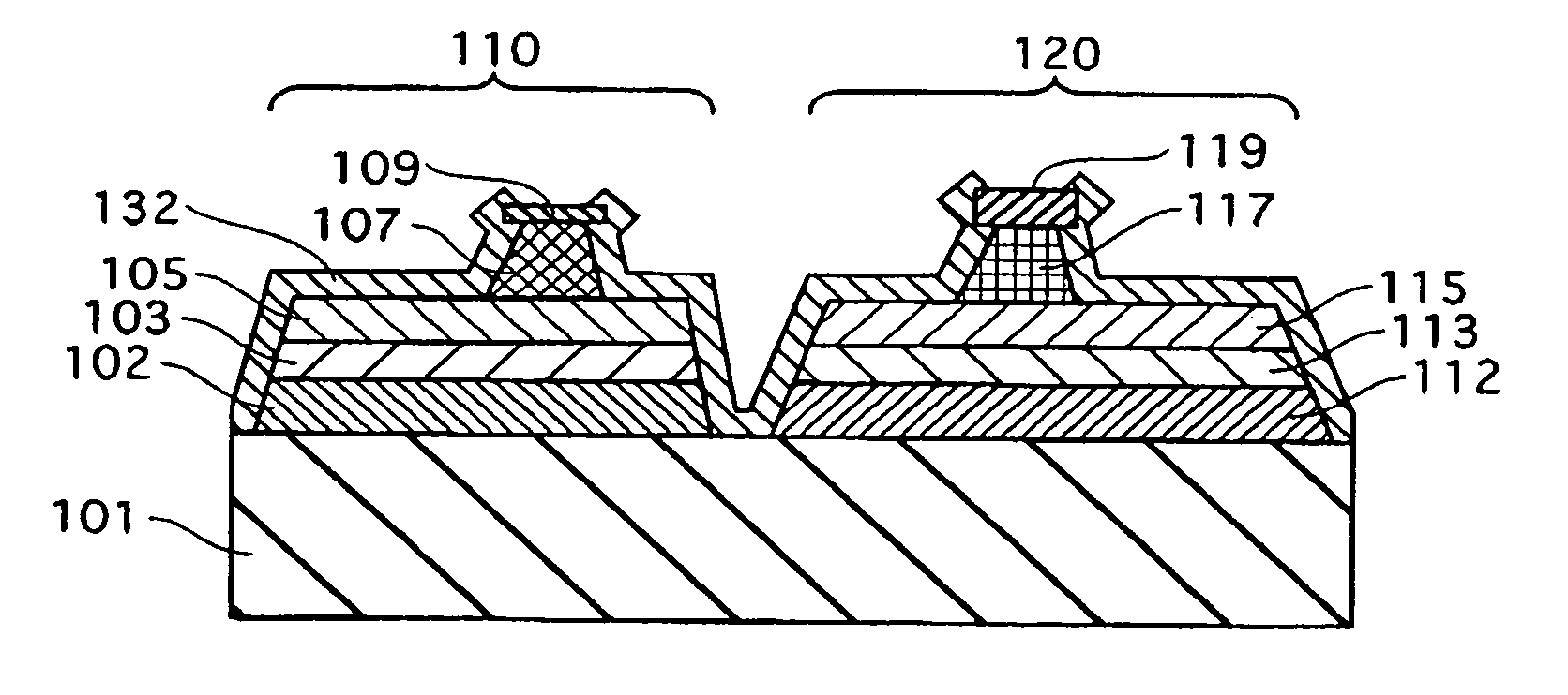
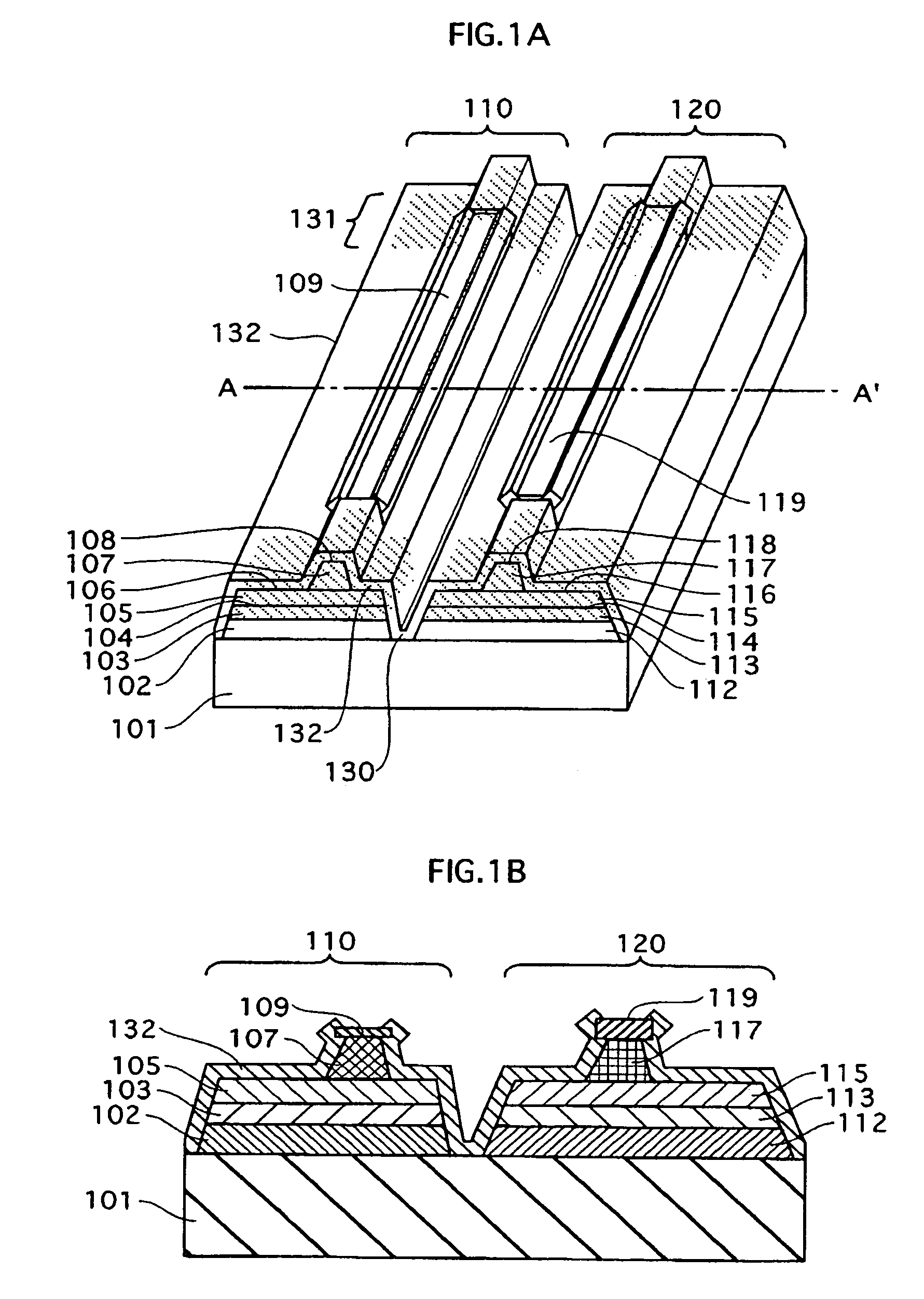
[0059]FIG. 1A is a schematic oblique view of a semiconductor laser device according to an embodiment 1 of the present invention. FIG. 1B is a sectional view taken along the line A-A′ of FIG. 1A.

[0060]According to the embodiment, the monolithic dual-wavelength semiconductor laser device is composed of an n-type GaAs substrate 101, and an infrared laser element 110 and a red laser element 120 assembled on the substrate 101. Each laser element has the following construction.

[0061]The infrared laser element 110 has the following layers laminated on the n-type GaAs substrate 101 in the stated order: an n-type GaAs buffer layer 102; an n-type (AlxGa1-x)yIn1-yP cladding layer 103; a GaAs / AlGaAs-based active layer 104; a p-type (AlxGa1-x)yIn1-yP first cladding layer 105; a p-type GaInP etching stop layer 106; a p-type (AlxGa1-x)yIn1-yP second cladding layer 107 having a ridge shape; a p-type GaInP intermediate layer 108; and a p-type Ga...

embodiment 2

[0116]FIG. 6A is an oblique view of a semiconductor laser device according to an embodiment 2 of the present invention. FIGS. 6B and 6C are sectional views of the semiconductor laser device.

[0117]The semiconductor laser device of the embodiment 2 is basically similar in construction to the semiconductor laser device of the embodiment 1. The difference lies in that the current blocking layer is made of AlInP. In addition the manufacturing method differs from that of the embodiment 1. The following describes the second manufacturing method with reference to FIGS. 5 and 6.

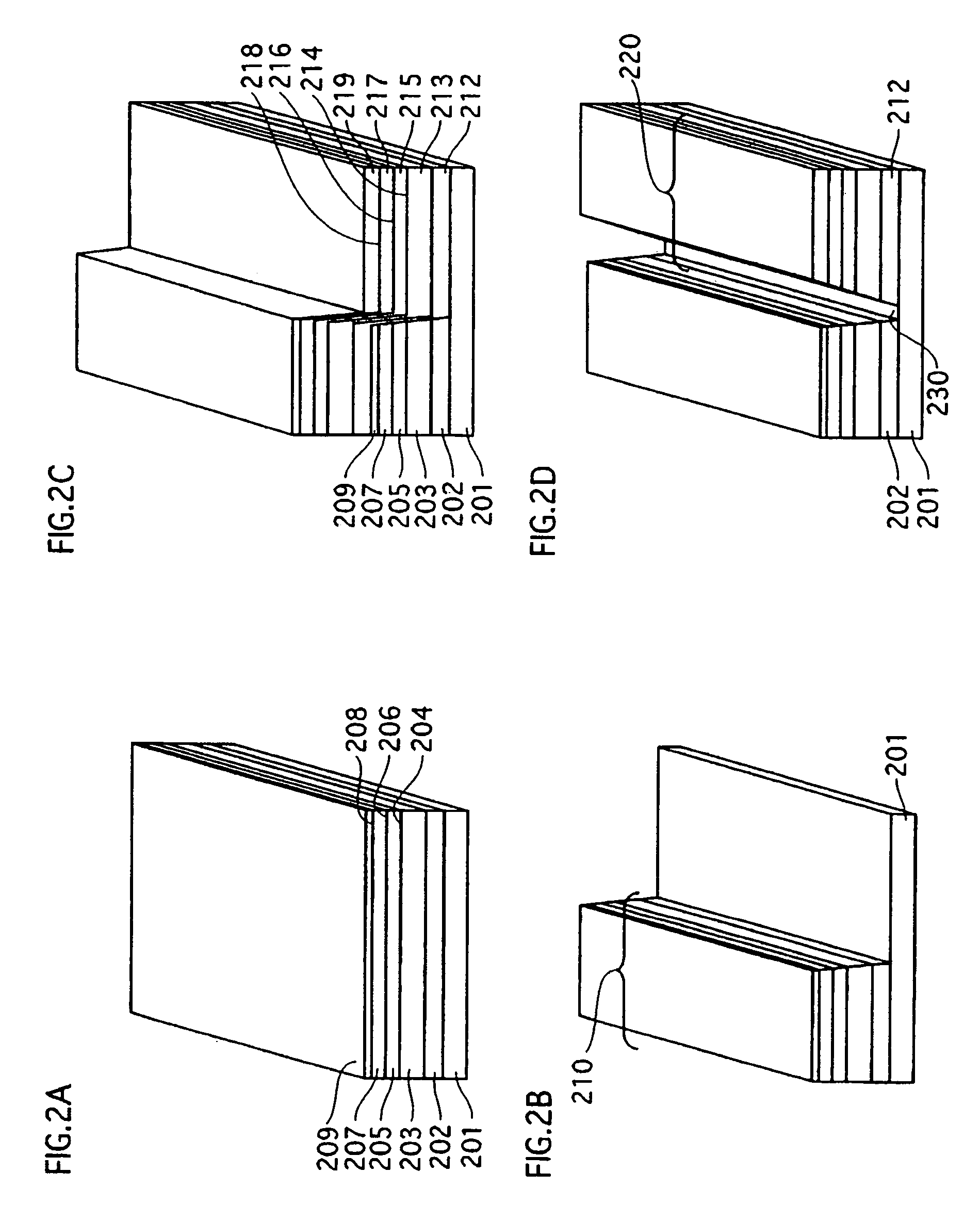
[0118]Through the same steps illustrated in FIGS. 2A-3B of the embodiment 1, the ridges constituting part of the waveguides are formed.

[0119]Next, as illustrated in FIG. 5A, the SiO2 film (not illustrated) and contact layers 309 and 319 are etched using photolithography to remove regions thereof existing above window structures 331.

[0120]Next, as illustrated in FIG. 5B, AlInP is selectively grown to form a current blo...


PUM


Abstract

In a monolithic dual-laser semiconductor laser device capable of high power output, a window structure for each of laser elements is formed through a common step, thereby improving the device reliability. The semiconductor laser device has an infrared laser element li0 and a red laser element 120 monolithically integrated on an n-type semiconductor substrate i01. Each of the infrared and red laser elements 110 and 120 has a ridged waveguide and a window structure formed by Zn diffusion at each resonator facet. The infrared and red laser elements ii0 and 120 include p-type contact layers 109 and 119 on the ridges of the respective waveguides. The p-type contact layer 109 is thinner than the p-type contact layer 119.

Description

[0001]This application is based on an application No. 2004-283887 filed in Japan, the contents of which are hereby incorporated by reference.BACKGROUND OF THE INVENTION[0002](1) Field of the Invention[0003]The present invention relates to a semiconductor laser device and a manufacturing method thereof. More particularly, the present invention relates to a monolithic dual-wavelength semiconductor laser device having two semiconductor lasers of mutually different oscillation wavelengths, and to a manufacturing method thereof.[0004](2) Description of the Related Art[0005]In recent years, large capacity DVD drives for recording and playback of optical information are rapidly becoming common in various fields, most notably in the field of video players. It is strongly desired that DVD drives be capable of reading conventional recording media, such as CDs, CD-Rs, and CD-RWs. To satisfy the demand, a DVD drive has two light sources for an optical pickup to record and play back DVDs and CDs...

Claims


Application Information

Patent Timeline
Patent Type & Authority Patents(United States)
IPC IPC(8): H01S5/00
CPCB82Y20/00H01S5/162H01S5/0425H01S5/22H01S5/34313H01S5/34326H01S5/4031H01S5/4087H01S5/02461H01S5/0421
Inventor KASHIMA, TAKAYUKIMAKITA, KOUJIYOSHIKAWA, KENJI
Owner PANASONIC CORP
Why Eureka
Try Eureka