Comparison device and analog-to-digital converter

Active Publication Date: 2009-03-31
IND TECH RES INST
View PDF8 Cites 12 Cited by
  • Summary
  • Abstract
  • Description
  • Claims
  • Application Information

AI Technical Summary

Benefits of technology

[0009]Accordingly, the present invention is a comparison device with calibration and an analog-to-digital converter (ADC) using the same. The comparison device corrects the offset voltage of the comparators with no assumption on input signal statistics and is useful for high-speed ADC, especially flash ADC. The ADC using the

Problems solved by technology

The intrinsic limitations of the flash ADC 100 are the process variation of a reference ladder resistance, the mismatch among the 2N−1 signal paths, and the threshold mismatch among the comparators.
However, the ADC power efficiency is

Method used


Image

  • Comparison device and analog-to-digital converter
  • Comparison device and analog-to-digital converter
  • Comparison device and analog-to-digital converter

Examples


Example

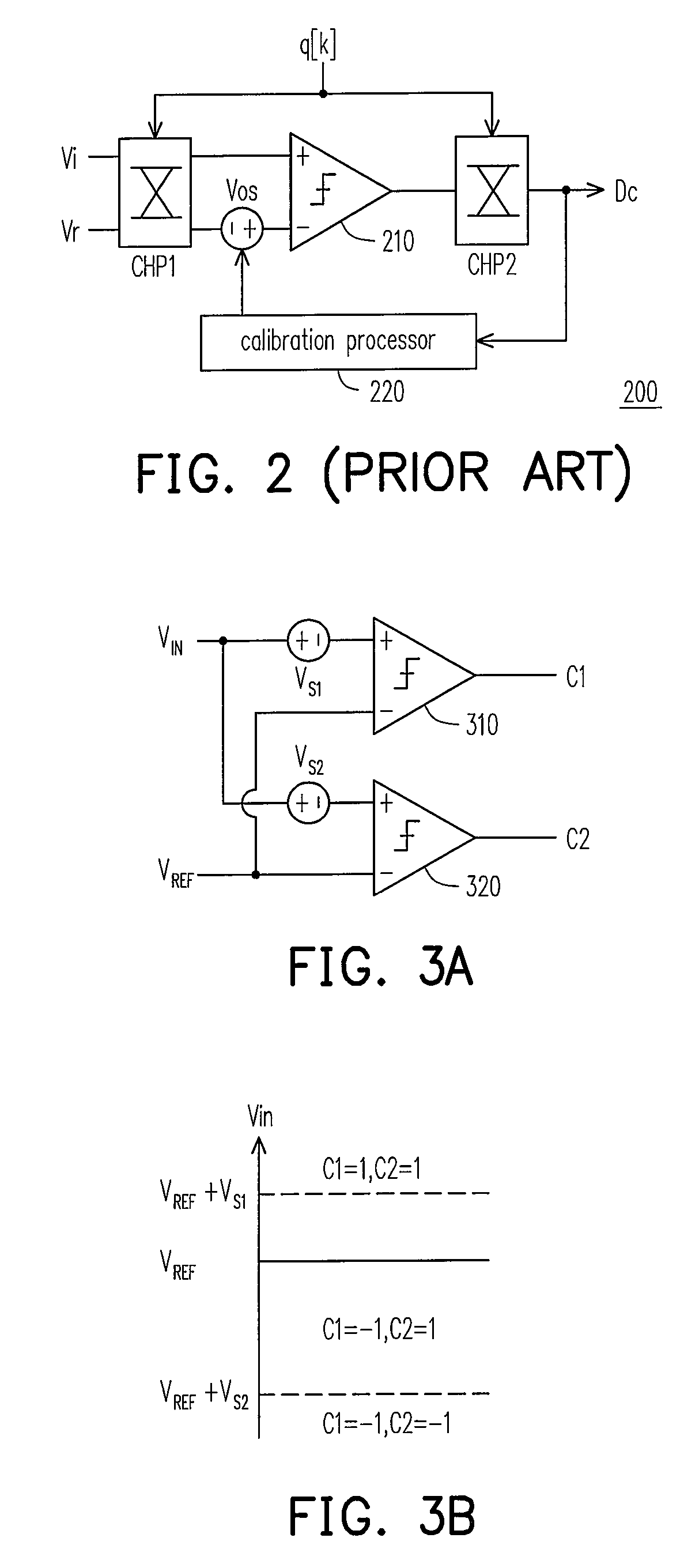
[0024]FIG. 3A is a circuit diagram of two comparators with the same input signal VIN and the reference voltage VREF. FIG. 3B is a diagram of the output signals of the comparators with offset voltages versus the input signal in FIG. 3A. Referring to FIG. 3A and FIG. 3B, the comparators 310 and 320 have different offset voltages VS1 and VS2 respectively, that is, the threshold voltage VT1 of the comparator 310 equals (VREF+VS1), and the threshold voltage VT2 of the comparator 320 equals (VREF+VS2). It is assumed that the threshold voltage VT1 is greater than the threshold voltage VT2. If the input signal VIN is greater than (VREF+VS1), the output signal C1 of the comparator 310 has logic high level (“1”), so does the output signal C2 of the comparator 320. If the input signal VIN is less than the (VREF+VS2), the output signal C1 of the comparator 310 has logic low level (“−1”), so does the output signal C2 of the comparator 320. While the input signal VIN falls between the two thresho...


PUM


Abstract

The comparison device includes a first through second comparators, a chop switching unit, a delta-sigma modulation unit, and a first through second compensation units. The chop switching unit transmits a first and a second signals to two input terminals of the first comparator during a first period, and inverses the first and second signals during a second period. The delta-sigma modulation unit compares the comparison results of two parallel comparators and generates the digital control codes for the comparators with the awareness of the chop switching unit. The first and the second compensation units adjust the threshold voltages of the comparators according to the digital control codes and a step size for calibrating the offset voltages of two comparators. The calibration scheme requiring no assumption on the input signal statistics is background thus the comparison device will not interrupt normal operation and is immune to PVT variations.

Description

BACKGROUND OF THE INVENTION[0001]1. Field of the Invention[0002]The present invention relates to a comparison device and an analog-to-digital converter using the same adaptive background calibration scheme, and more particularly, to a device with adaptive background calibration scheme that can eliminate an offset voltage of the comparators.[0003]2. Description of Related Art[0004]With the continuous increase of communication network bandwidth, a conversion rate of a front-end analog-to-digital converter (ADC) must be increased for the requirements of an overall system. A flash ADC is the most popular architecture to implement high sampling rate ADC. FIG. 1 is a circuit diagram of the flash ADC. Referring to FIG. 1, the flash ADC 100 consists of 2N−1 comparators for comparing the sampled signal Vi with different reference voltages Vr, and also consists of encoder 110 for performing the bubble prevention and converting the thermal codes to the binary codes. The intrinsic limitations o...

Claims


Application Information

Patent Timeline
IPC IPC(8): H03M1/12
CPCH03K5/24H03M1/1019H03M1/362
Inventor LIU, WEN-BOHSIEN, SZU-KANGCHIU, YUN
Owner IND TECH RES INST
Why Eureka
Try Eureka