Surface acoustic wave element, surface acoustic wave device and communication device including the same

a technology of surface acoustic wave and surface acoustic wave, which is applied in the direction of device details, electrical equipment, and devices, etc., can solve the problems of unbalanced input or output, unbalanced input-output type surface acoustic wave filter, and unbalanced so as to reduce insertion loss and vswr, and minimize the deterioration of amplitude balance. ,

Active Publication Date: 2009-04-14
KYOCERA CORP
View PDF11 Cites 13 Cited by
  • Summary
  • Abstract
  • Description
  • Claims
  • Application Information

AI Technical Summary

Benefits of technology

[0044]With the foregoing background, it is an object of the present invention to provide a surface acoustic wave element that functions as a high quality surface acoustic wave filter with reduced insertion loss and VSWR by minimizing deterioration of amplitude balance and phase balance of surface acoustic wave element, a surface acoustic wave device and a communication device using the same.
[0046]In this structure, disposing the first and second reference potential terminals asymmetrically is equivalent to a condition where inductance components are connected to reference potential terminals of the surface acoustic wave element. Accordingly, this structure has the same effect as in the case where a matching circuit is connected to connecting terminals, so that the insertion loss and VSWR of the surface acoustic wave element can be reduced.
[0047]When one of a couple of comb-shaped electrodes of the odd number of IDT electrodes constituting the IDT electrode located at the center is separated into at least two parts, and connecting terminals are connected to each of the separated comb-shaped electrodes, a surface acoustic wave device including the surface acoustic wave element mounted on a mounting board can have the function of an unbalanced-balanced converter. In addition, since there is no parasite capacitance added on the connecting terminal side of the surface acoustic wave device with this structure, deterioration of the amplitude balance degree and phase balance degree can be reduced.
[0056]According to this structure, in the surface acoustic wave device including the surface acoustic wave element mounted on the mounting board, disposing the first and second ground conductors asymmetrically has the same effect as in the case where a matching circuit is connected to connecting terminals. This reduces deterioration of the amplitude balance degree and phase balance degree of this surface acoustic wave device, and as a result, the insertion loss and VSWR of the surface acoustic wave device can be reduced.
[0060]As discussed above, by applying a surface acoustic wave device of the present invention to a duplexer of a communication device, it is possible to provide a communication device with good radio frequency characteristics.

Problems solved by technology

One of such functions is an unbalanced-balanced conversion function which allows the surface acoustic wave filter to be constructed as unbalanced input-balanced output type or balanced input-unbalanced output type.
On the other hand, unbalanced input or unbalanced output refers to input or output of signal as an electrical potential of one signal line with respect to the ground potential.
A major part of conventional surface acoustic wave filters are unbalanced input-unbalanced output type surface acoustic wave filters (hereinafter, simply referred to as “unbalanced type surface acoustic wave filter”).
Also, when circuits and electronic components in stages prior to an unbalanced type surface acoustic wave filter are of balanced output type, a balun is required between the prior stages and the unbalanced type surface acoustic wave filter.
However, such a structure has a drawback that the balance degree is prone to deteriorate.
As a result, this surface acoustic wave element fails to achieve a sufficient balance degree.

Method used


Image

  • Surface acoustic wave element, surface acoustic wave device and communication device including the same
  • Surface acoustic wave element, surface acoustic wave device and communication device including the same
  • Surface acoustic wave element, surface acoustic wave device and communication device including the same

Examples


example

[0228]An example of a surface acoustic wave device according to the present invention will be hereinafter described.

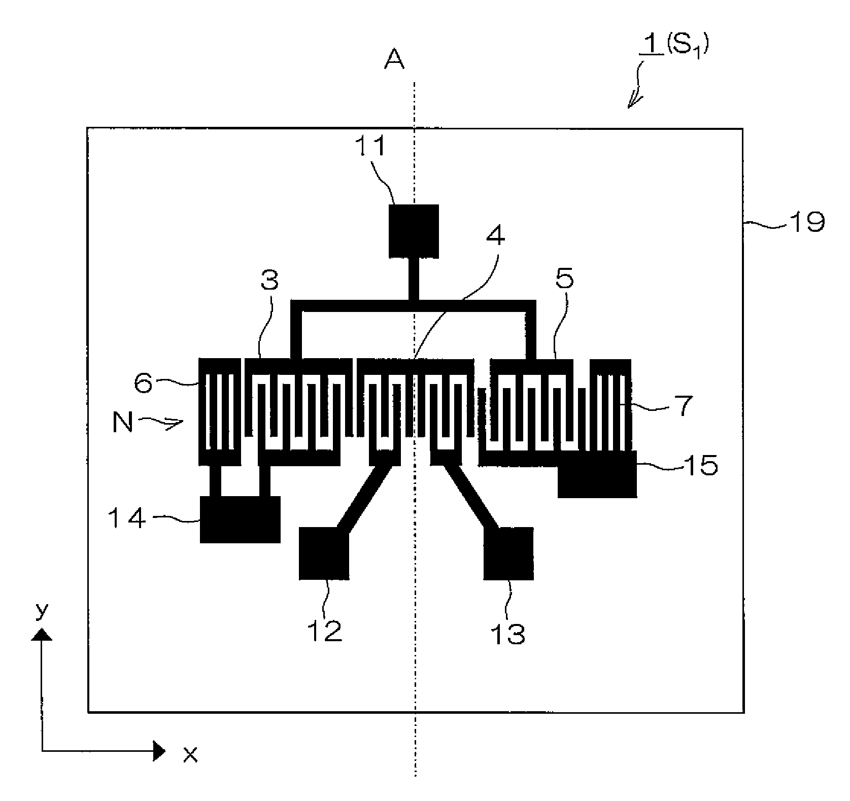
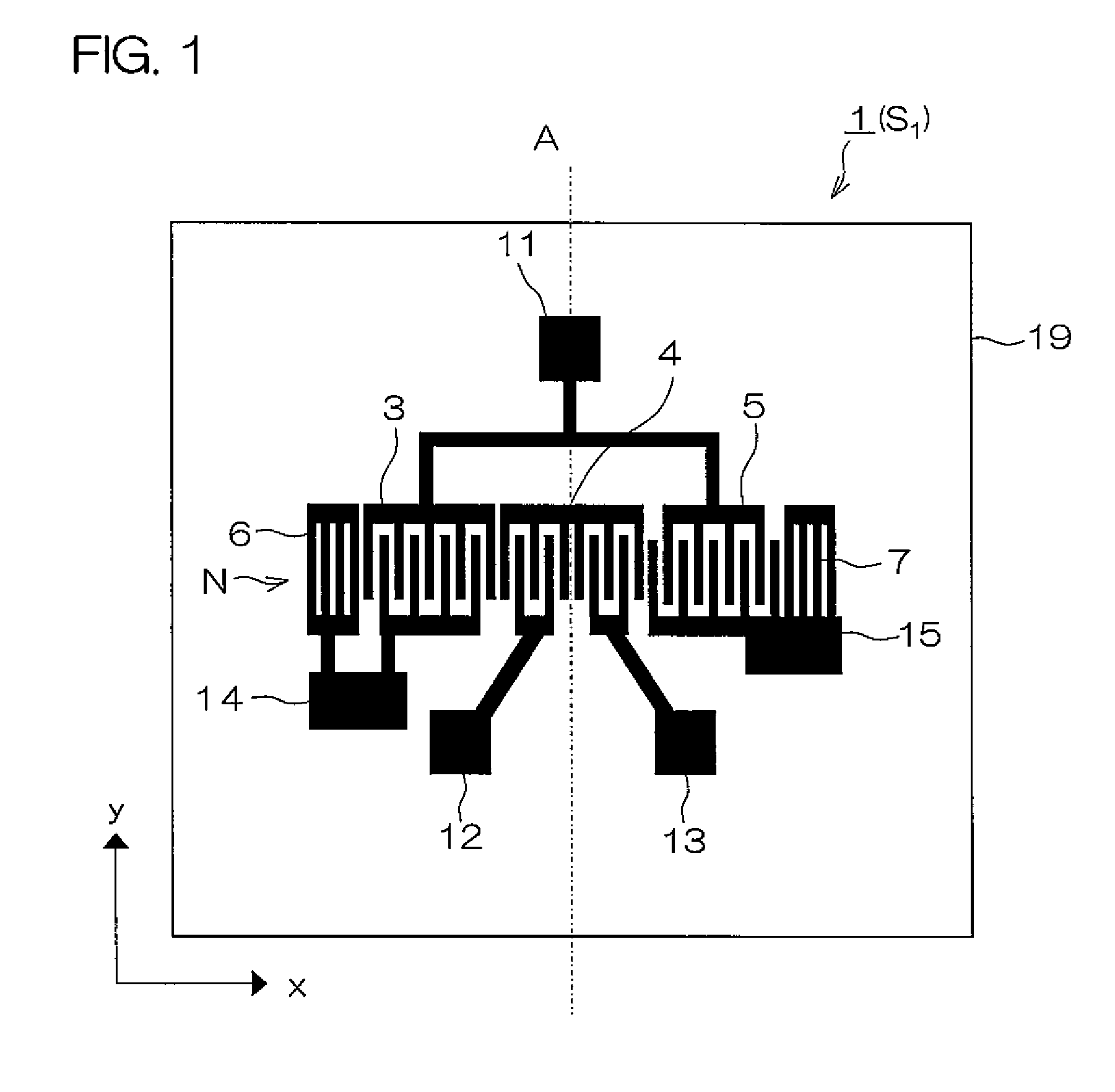
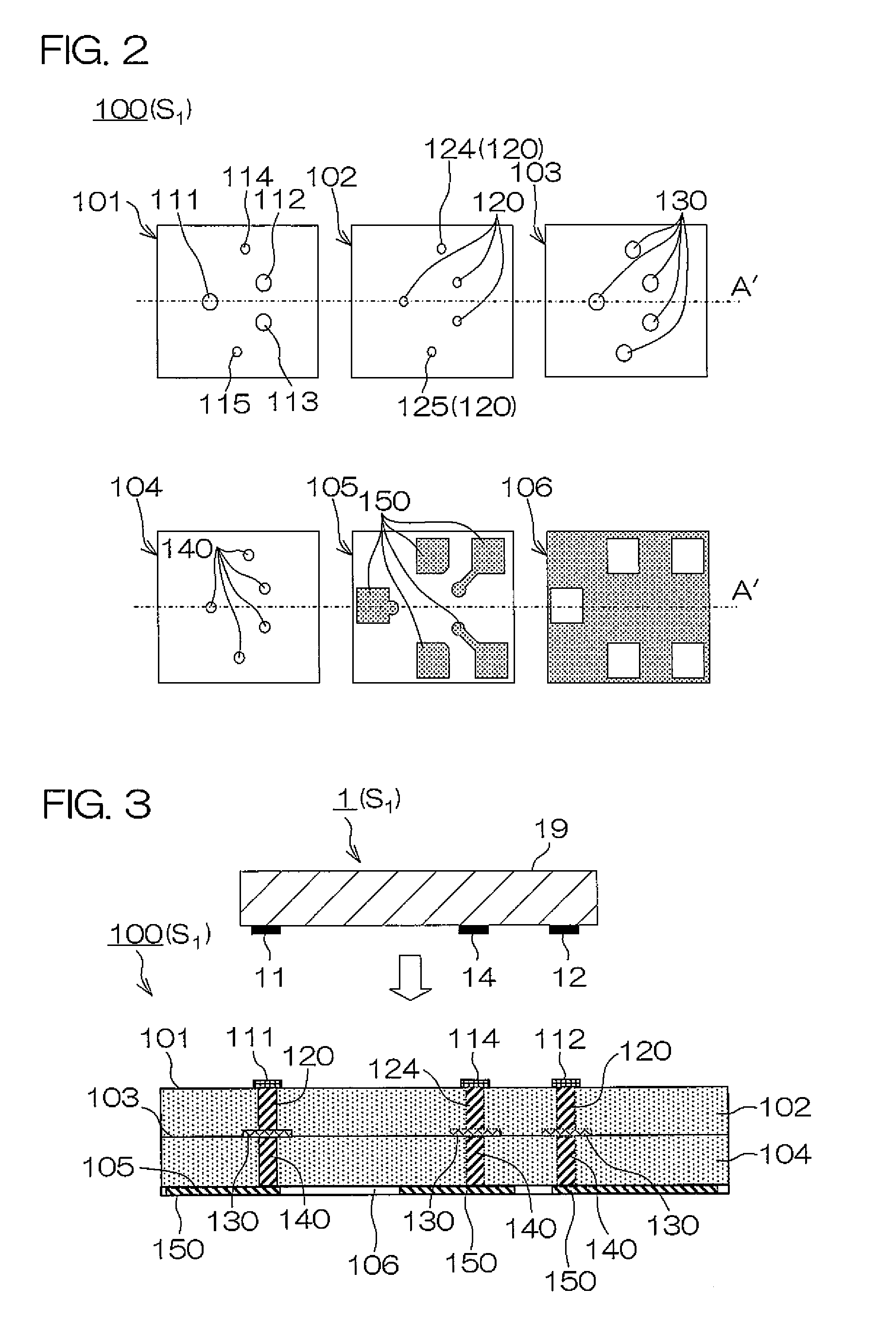
[0229]The surface acoustic wave device S1 including the surface acoustic wave element 1 shown in FIG. 1 mounted on the mounting board 100 shown in FIG. 2 is described in detail.

[0230]In this Example, a surface acoustic wave device S1 designed for the PCS (Personal Communication Service) having a center frequency in the 1800 MHz band used for mobile communication devices was produced.

[0231]First, a 38.7°-rotated Y-cut X-propagation LiTaO3 single crystal was used to produce a base substrate. The “base substrate” refers to a substrate before being diced (cut) into individual piezoelectric substrates 19.

[0232]Then, the electrode patterns including IDT electrodes 3-5, reflector electrodes 6, 7, connecting wires, terminals 11-15 to be formed on the individual piezoelectric substrates 19 of the base substrate were formed by photolithography using a sputtering apparatus, Step ...


PUM


Abstract

A surface acoustic wave element 1 comprises a piezoelectric substrate 19, IDT electrodes 3, 4, 5 of an odd number not less than three formed along a propagation direction of surface acoustic waves that propagates on the piezoelectric substrate, wherein IDT electrodes 3, 5 of the odd number of IDT electrodes 3, 4, 5 disposed on both sides of an IDT electrode 4 that is located at the center are connected to first and second reference potential terminals 14, 15, respectively, and the first and second reference potential terminals 14 and 15 are formed asymmetrically with respect to a virtual central axis A that passes through the center of the IDT electrode 4 located at the center and provided in a direction perpendicular to the propagation direction.

Description

BACKGROUND OF THE INVENTION[0001]1. Field of the Invention[0002]The present invention relates to a surface acoustic wave element, surface acoustic wave device, and a communication device including the same. The surface acoustic wave element according to the present invention includes surface acoustic wave filter elements, surface acoustic wave resonators and the like. The surface acoustic wave device according to the present invention is used for mobile communication devices such as portable phones.[0003]2. Description of the Related Art[0004]Surface acoustic wave filters have been widely used as bandpass filters used for the RF (Radio Frequency; wireless frequency) stages of mobile communication devices including portable phones, automobile telephones and the like. In addition to miniaturization, adapting to wider passband and higher frequency supporting communications carriers, improvement of out-of-passband attenuation and insertion loss within the passband are required for these...

Claims


Application Information

Patent Timeline
Patent Type & Authority Patents(United States)
IPC IPC(8): H03H9/00H03H9/205H01L41/02
CPCH03H9/0038H03H9/0057H03H9/008H03H9/14588
Inventor MAKIBUCHI, DAISUKEOTSUKA, KAZUHIROIIOKA, KIYOHIRO
Owner KYOCERA CORP
Why Eureka
Try Eureka