Flash memory device including a dummy cell

a flash memory and dummy cell technology, applied in the field of semiconductor memory devices, can solve the problems of reducing the cost of the ssd, affecting the capacity and cost, and increasing the capacity

Active Publication Date: 2009-04-14
SAMSUNG ELECTRONICS CO LTD
View PDF19 Cites 66 Cited by
  • Summary
  • Abstract
  • Description
  • Claims
  • Application Information

AI Technical Summary

Problems solved by technology

While a SSD is considered to be inferior in capacity and cost to the HDD, the SSD is considered to be superior in access speed, miniaturization, and durability of percussion to the HDD.
Moreover, it is expected that the progress of design and process technologies may increase the capacity and decrease the cost of the SSD.
While an increase in the integration density of memory cells in a semiconductor device may help reduce the size of the device, an increase in integration density may also cause problems.
This programming of program-inhibit cells is generally undesirable.
While the above-mentioned self-boosting scheme may be used to program-inhibit a memory cell, this scheme may not work as well in a high integration density memory device.
This increase in the potential difference between the gate and channel may lead to an undesirable programming operation.
Thus, because of the relatively large coupling ratio between unselected world lines and a selected word line, it may be undesirable to apply the local self boosting scheme to a highly integrated flash memory.
This drop in the channel voltage of the cell transistor MC30> may lead to an undesirable programming operation due to increase in a voltage difference between the gate and the channel.
The above-mentioned drawback may become an important issue in a NAND flash memory device which starts a programming operation from a word line WL0> in an ascending order.

Method used


Image

  • Flash memory device including a dummy cell
  • Flash memory device including a dummy cell
  • Flash memory device including a dummy cell

Examples


Embodiment Construction

[0030]The present invention will now be described more fully hereinafter with reference to the accompanying drawings, in which preferred embodiments of the invention are shown. This invention, however, may be embodied in many different forms and should not be construed as limited to the embodiments set forth herein. Rather, these embodiments are provided so that this disclosure will be thorough and complete, and will fully convey the scope of the invention to those skilled in the art.

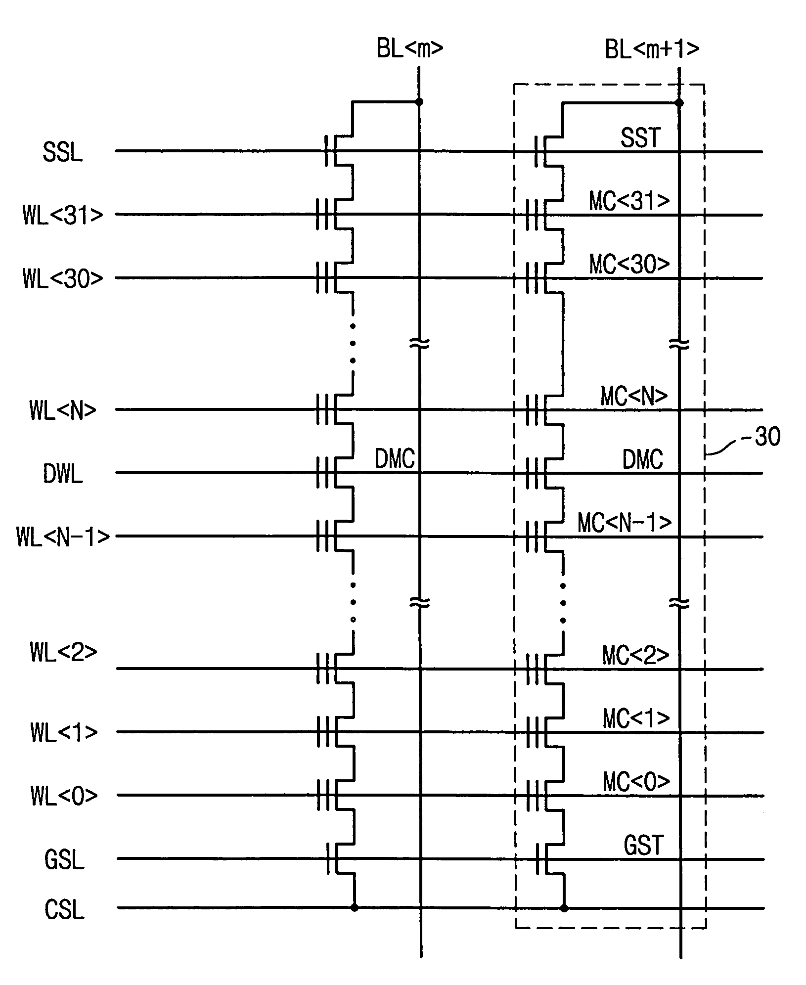
[0031]FIG. 4 shows a schematic circuit diagram of an array structure according to an exemplary disclosed embodiment. Referring to FIG. 4, a dummy cell DMC is placed in each of strings 30. In each string 30, the dummy cell DMC blocks the sharing of charges being boosted in a channel of a program-inhibited cell. Furthermore, in each of the strings 30, the dummy cell DMC has the same characteristics and performance as other memory cells in a corresponding sting. Generally, each of the strings includes 32 m...


PUM


Abstract

A nonvolatile semiconductor memory device includes a string selection transistor coupled to a bit line. The device also includes a plurality of memory cells coupled in series to the string selection transistor, wherein at least one of the memory cells is configured to be in a programmed state during an erase procedure of the plurality of memory cells.

Description

BACKGROUND OF THE INVENTION[0001]1. Field of the Invention[0002]The present invention relates to a semiconductor memory device and, in particular, to a NAND flash memory device that includes a dummy cell.[0003]This U.S. non-provisional patent application claims priority under 35 U.S.C § 119 to Korean Patent Application 2006-002310 filed on Jan. 09, 2006, the disclosure of which is hereby incorporated by reference in its entirety.[0004]2. Description of the Related Art[0005]Generally, NAND flash memory devices are programmed and erased using Fowler-Nordheim (F-N) tunneling. In F-N tunneling, electrons are injected / discharged from / to a channel region into / from a floating gate due to a large voltage difference between the channel region and a control gate of a cell transistor. Because of the relative ease in programming and erasing NAND flash memory devices, NAND flash memory devices are known to have good data storage characteristics as compared to other non-volatile memory devices. M...

Claims


Application Information

Patent Timeline
Patent Type & Authority Patents(United States)
IPC IPC(8): G11C11/34
CPCG11C11/5621G11C16/0483A01K5/02A01K7/025A01K5/0142
Inventor KANG, SANG-GU
Owner SAMSUNG ELECTRONICS CO LTD
Why Eureka
Try Eureka