Memory circuit, method for operating a memory circuit, memory device and method for producing a memory device

a memory circuit and circuit technology, applied in the field of memory circuits, can solve the problems of reducing resistance, unable to detect the logic state to which the resistance state is associated correctly, and unable to detect stored information correctly

Inactive Publication Date: 2009-04-21
POLARIS INNOVATIONS LTD
View PDF11 Cites 0 Cited by
  • Summary
  • Abstract
  • Description
  • Claims
  • Application Information

AI Technical Summary

Benefits of technology

[0006]One embodiment of the present invention a memory device including resistive memory cells is provided to avoid a degradation of the resistance state to which a resistive memory element is set due to disturbances induced from neighbored signal lines can be avoided.
[0007]A further embodiment of the present invention provides a method for operating such a memory device. Furthermore, another embodiment of the present invention provides a memory device which provides protection against signal disturbances at the node between the selection transistor and the resistive memory element which can easily be produced, and a method for producing such a memory device.
[0009]According to a first aspect a memory circuit is provided which comprises a resistive memory element including a programmable metallization cell, a bit line, a selection transistor to address the resistive memory element coupling the resistive memory element to the bit line and a further transistor coupled to the resistive memory element applying a predefined potential at a node between the selection transistor and the resistive memory element. Thereby, it can be achieved that the node between the selection transistor and the resistive memory element is hold on the predefined potential at least at the time when the selection transistor is non-conductive so that no floating of the node can occur which may result in a change of the resistance state of the resistive memory element.

Problems solved by technology

Such disturbances may result in an undesired voltage drop over the resistive memory element which can reduce the resistance of the resistive memory element.
A change of the resistance of the resistive memory element may result in that the logic state to which the resistance state is associated cannot be detected correctly.
Even if the voltage drop over the resistive memory element is not sufficient to program the resistive memory element to a low resistance state, repeated appliance of the voltage drops over the resistive memory element can cause a change in the resistance so that after a plurality of accesses of the respective memory cell the stored information cannot be detected correctly.
Even if the stored information can be detected correctly after a change of the resistance of the resistive memory element such a reduction of the resistance may further result in a prolongation of the access time on the memory cell.

Method used


Image

  • Memory circuit, method for operating a memory circuit, memory device and method for producing a memory device
  • Memory circuit, method for operating a memory circuit, memory device and method for producing a memory device
  • Memory circuit, method for operating a memory circuit, memory device and method for producing a memory device

Examples


Embodiment Construction

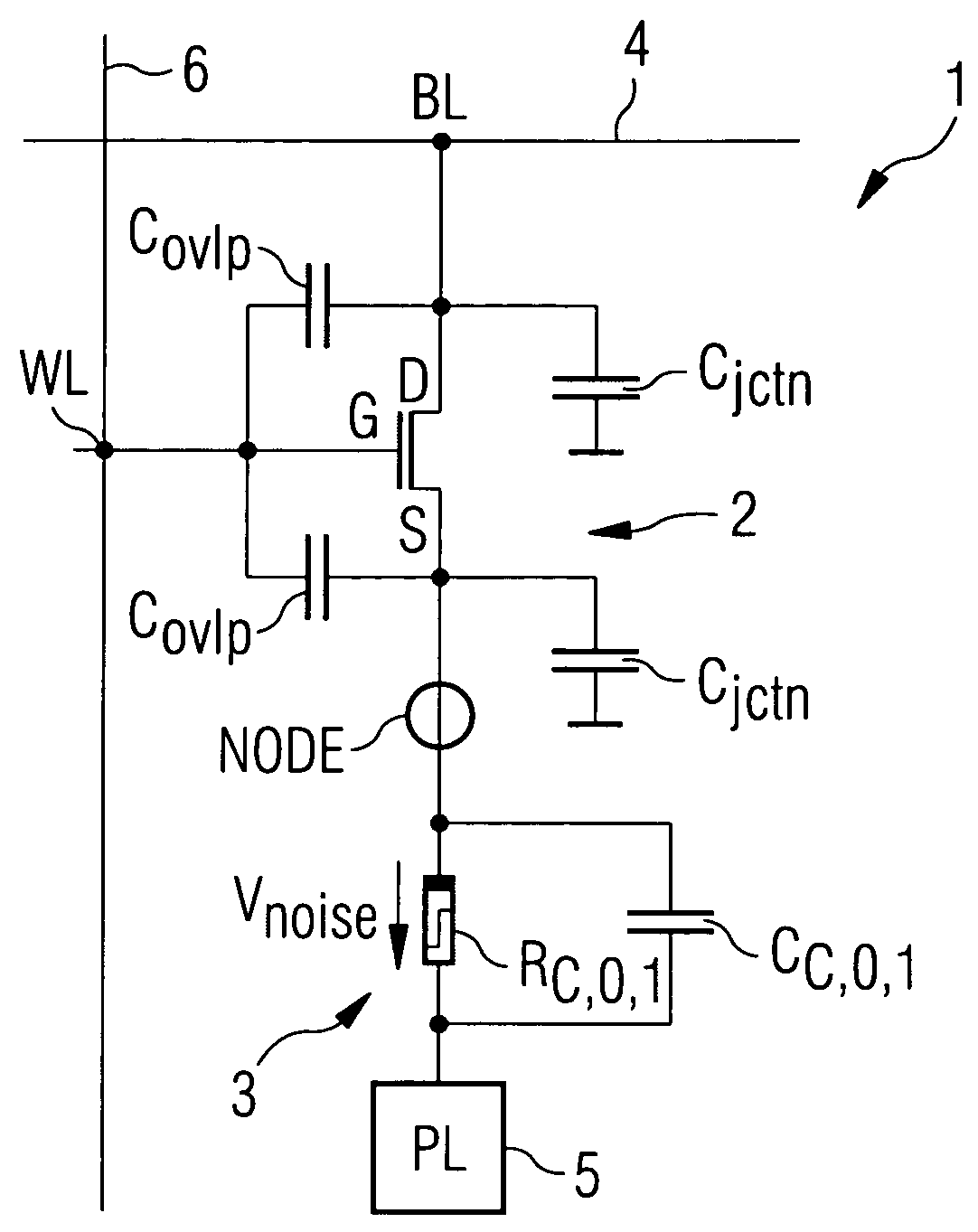
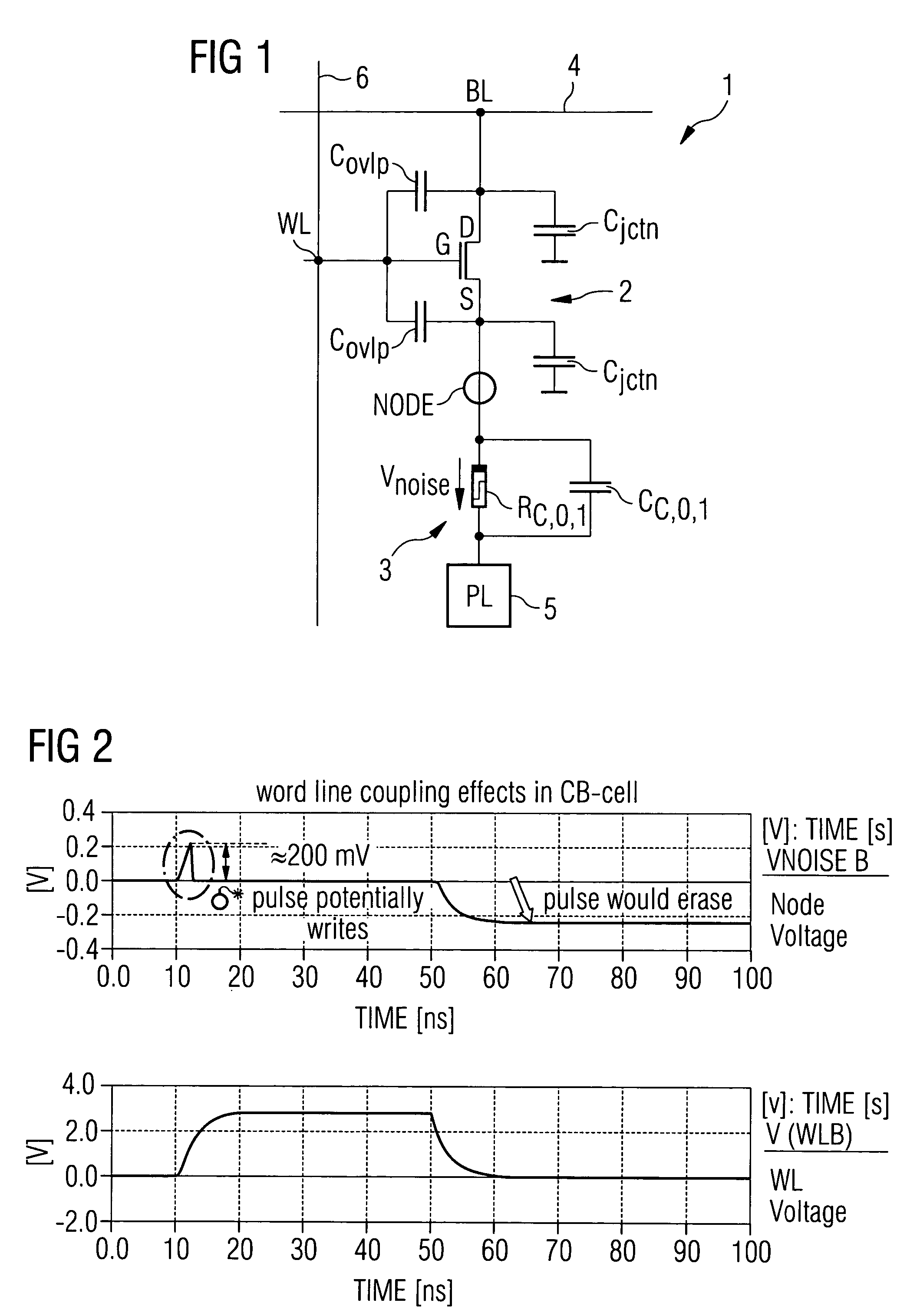
[0023]In FIG. 1 a schematic diagram of a resistive memory cell 1 as used in a memory device is shown. The resistive memory cell 1 comprises a selection transistor 2 and a resistive memory element 3 which are coupled in series between a bit line 4 and a plate element 5. The plate element 5 supplies a predetermined plate potential which is set to a fixed potential value. In detail, a first terminal of the selection transistor 2 is coupled to the bit line 4 and a second terminal of the selection transistor 2 is coupled with a first terminal of the resistive memory element 3. A second terminal of the resistive memory element 3 is coupled to the plate element 5. A gate terminal of the selection transistor 2 is coupled to a word line 6 on which an activation signal can be applied to render the selection transistor 2 conductive or non-conductive.

[0024]The resistive memory element 3 is configured as a CBRAM memory element which has a solid state electrolyte material which is sandwiched betw...


PUM


Abstract

The present invention is related to a memory circuit comprising: a resistive memory element comprising a programmable metallization cell, a bit line, a selection transistor operable to address the resistive memory element for coupling the resistive memory element to the bit line, and a further transistor coupled with the resistive memory element for applying a predefined potential at a node between the selection transistor and the resistive memory element.

Description

BACKGROUND OF THE INVENTION[0001]1. Field of the Invention[0002]The present invention relates to a memory circuit comprising a resistive memory element and a method for operating such a memory circuit. The present invention further relates to a memory device in which a resistive memory element is integrated and a method for producing such a device.[0003]2. Description of the Related Art[0004]Memory devices may comprise resistive memory elements for storing information. The resistive memory element can acquire different resistance states each of which may be associated with a logic state. Resistive memory elements are known as CBRAM memory elements (CBRAM: conductive bridging RAM), PMC memory elements (PMC: programmable metallization cell) or other terms may be used. A resistive memory element as understood in the present invention may include a solid state electrolyte which is sandwiched between an anode made from a migrating material and an inert cathode. By applying an electrical ...

Claims


Application Information

Patent Timeline
Patent Type & Authority Patents(United States)
IPC IPC(8): G11C11/00
CPCG11C13/0011G11C13/003G11C2213/75G11C2213/76G11C2213/79
Inventor LIAW, CORVINHOENIGSCHMID, HEINZBRUCHHAUS, RAINER
Owner POLARIS INNOVATIONS LTD
Why Eureka
Try Eureka