Apparatus and method for transmitting and receiving high-speed differential current data between circuit devices

a technology of differential current and circuit devices, applied in the direction of baseband system details, power management, wireless communication, etc., can solve the problems of dominating the power consumption of the interface circuit and high transmit power, and achieve the effect of reducing the input impedance of the common-base amplifier emitter connection, reducing the total impedance, and increasing the bit error ra

Inactive Publication Date: 2009-04-21
UNIVERSITY OF DELAWARE
View PDF2 Cites 15 Cited by
  • Summary
  • Abstract
  • Description
  • Claims
  • Application Information

AI Technical Summary

Benefits of technology

[0008]In addition, the ability of the present invention to adjust transmit current level based on link distance is a key advantage of the present invention over the background art. High transmit current levels result in high transmit power that then dominates the power consumption of the interface circuit.
[0009]The present invention is an apparatus and method for transmitting and receiving high-speed differential current data between circuit devices. In particular, the apparatus comprises a driver circuit and receiver circuit that form an interface for transmitting and receiving differential high-speed signals over a transmission line. The transmission line is terminated at a receiver end by one end of a resistive element. The second end of the resistive element feeds a common base transistor amplifier and the base of a common emitter amplifier. The two amplifiers are connected so that the gain of the common emitter amplifier further lowers the input impedance of the common-base amplifier emitter connection. The common-base transistor amplifier converts the received signal current into a voltage on the collector, and the transmission line terminating resistive element is essentially unaffected by the connected amplifier circuits.
[0010]In accordance with a preferred embodiment, a differential current is transmitted over two transmission lines to a receiver. The receiver includes first and second resistive elements, each having one end connected to an input of a respective first and second common-base transistor amplifier. A differential amplifier has a first and second inputs connected, respectively, to the one end of first and second resistive elements. The collectors of the differential amplifier are connected to the bases of the first and second common-base transistor amplifiers. The effect is to reduce the total impedance seen by the first and second resistive elements so that the transmission line termination impedance is effectively the impedance of the first and second terminating resistive elements.
[0011]In accordance with another embodiment of the present invention, a driver circuit comprising a differential amplifier circuit produces first and second currents to drive first and second transmission lines. The operating voltage for running the driver circuit differential amplifier is obtained from the receiver circuit through the first and second transmission lines.
[0012]In the following paragraph, the terms drain and source are interchangeable to provide an alternative configuration of the present invention. Another embodiment of the present invention is An interface for transmitting and receiving differential currents transmitted over first and second transmission lines comprising: a driver circuit for supplying a differential current to said first and second transmission lines comprising: a differential amplifier circuit having first and second signal inputs connected to the base connections of first and second differential transistors, said transistors having collector connections connected to said transmission lines; a resistor connected between collector connections of said first and second differential transistors; and a current source connected to emitter connections of said differential transistors.
[0013]In addition, this embodiment further includes a receiver comprising: first and second resistive elements having one end connected to respective of said first and second transmission lines; a first common-gate amplifier connected to receive a second end of said first resistive element on a source connection thereof, and producing a voltage signal on a respective drain connection; a second common-gate amplifier connected to receive a second end of said second resistive element on a source connection thereof, and producing a voltage signal on a respective drain connection; a differential amplifier having first and second inputs connected, respectively, to said first and second resistive elements second ends; having first and second drains, respectively, connected to first and second sources, respectively, of a cascode amplifier; and having first and second sources connected to ground; first and second drain resistors connecting respective drains of said first and second common-gate amplifiers to a terminal of a power supply; and first and second active load transistors having first and second gates interconnected, having first and second sources, respectively, connected to first and second drains of said cascode amplifier and having said first and second drains connected to said power supply, wherein a differential current received by said first and second resistive elements is converted to a differential voltage on said common-gate amplifiers drain connections.

Problems solved by technology

High transmit current levels result in high transmit power that then dominates the power consumption of the interface circuit.

Method used


Image

  • Apparatus and method for transmitting and receiving high-speed differential current data between circuit devices
  • Apparatus and method for transmitting and receiving high-speed differential current data between circuit devices
  • Apparatus and method for transmitting and receiving high-speed differential current data between circuit devices

Examples


Embodiment Construction

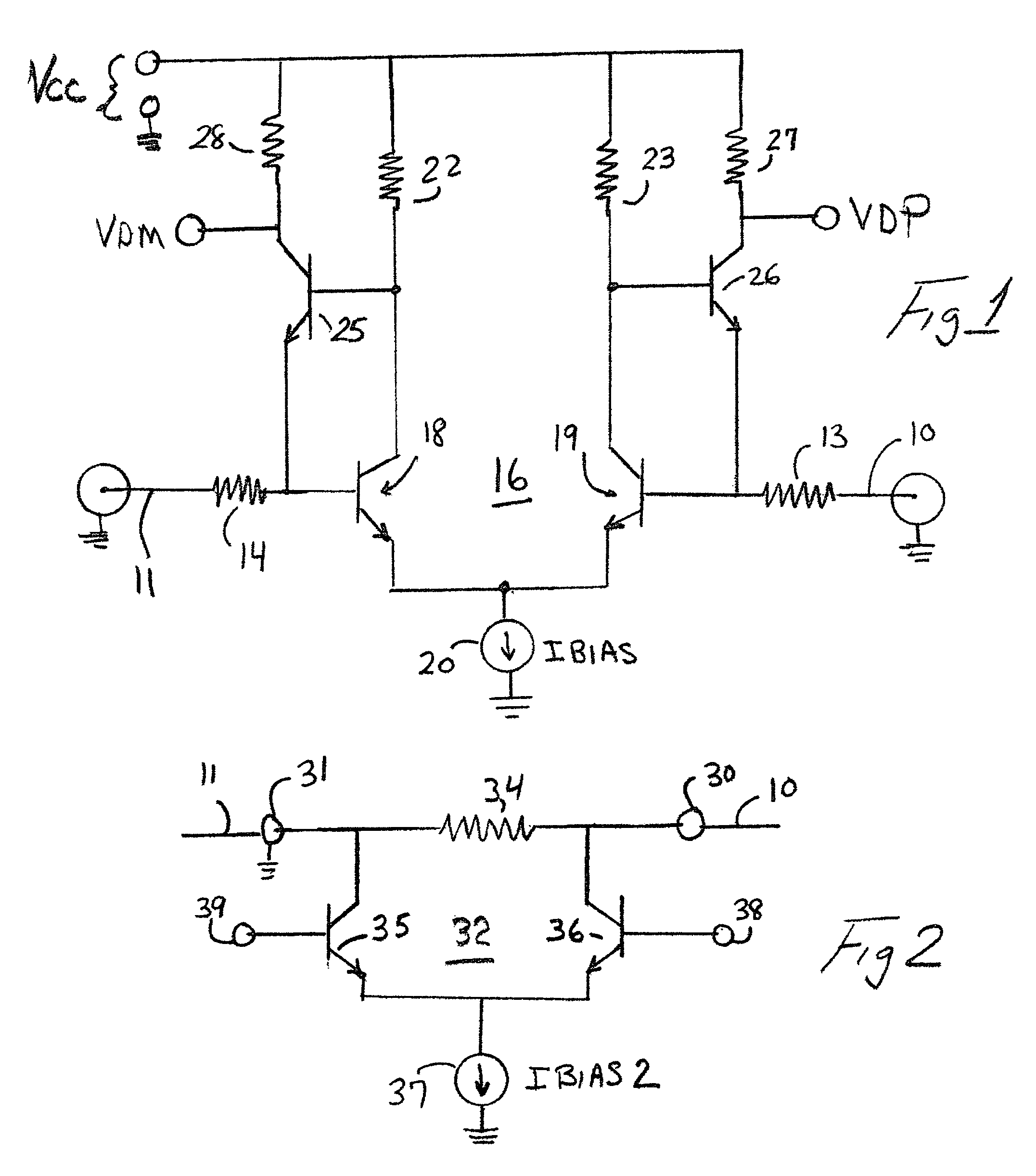
[0021]Referring now to FIG. 1, a receiver for high-speed differential digital signals is shown. Transmission lines 10, 11 carry differential digital signals from a driver circuit to one side of terminating resistances 13, 14, respectively. Terminating resistances 13 and 14 are selected to be as close in value to the characteristic impedance of the transmission lines 10 and 11 as possible. Transmission lines 10 and 11 can be for example, wire or other conductors that have a length that acts as a transmission line at the frequencies higher than 1 gigabit per second. It should be noted that lengths of wire or other conductors of just a few inches exhibit transmission line characteristics at these high frequencies.

[0022]Each of the terminating resistances 13 and 14 are connected to the emitters of a first and second common-base amplifier circuit 26, 25, respectively. The common-base amplifier circuits comprise transistors 25 and 26, and collector resistors 28 and 27, respectively. The i...


PUM


Abstract

An apparatus and method for an interface for transmitting high speed data between circuits. A driver circuit produces first and second differential currents from a digital signal that drive first and second transmission lines. A receiver is connected through first and second terminating resistors to said transmission lines. The resistive elements are in turn connected to first and second common base amplifiers where the differential currents are converted to a differential voltage. The input impedance to the first and second common-base amplifiers is further lowered by a differential amplifier having inputs connected to the inputs of the common-base amplifiers, and an output connected to the bases of said common-base amplifiers. As a result, voltage conversion of the differential signals takes place in the common-base amplifiers and not in the terminating resistors, reducing the level of the differential currents and permitting an increase in the digital data rate. In addition, a common-gate amplifier configuration of the present invention is provided as well as a method for dynamically determining an optimal transmit power level for the driver circuit and for performing an accelerated bit error rate measurement.

Description

GOVERNMENT RIGHTS[0001]This application is based on subject matter developed pursuant to DARPA Contract FA 8650-04-C-7120 / Subcontract 19779.BACKGROUND OF THE INVENTION[0002]The present invention provides a driver and a receiver circuit for transmitting high-speed data between electronic devices. Specifically, a receiver and associated driver circuit form an interface circuit for transferring data at high speeds between circuit devices.[0003]Battery operated, portable and handheld electronic devices such as, mobile phones, portable entertainment consoles, personal digital assistants (PDAs), global positioning systems (GPS) and gaming devices, are evolving to the point where internal data transfers may occur at rates in excess of 100 megabits per second. It is expected that such portable and handheld devices are likely to require internal data transfers in excess of 1 gigabit per second. These faster data rates represent an increase of 10 to 100 times over current data transfer rates ...

Claims


Application Information

Patent Timeline
Patent Type & Authority Patents(United States)
IPC IPC(8): H04B3/00H04L25/00
CPCH04L25/0274H04L25/0292H04W52/20
Inventor KIAMILEV, FOUADKRAMER, JOSHUAZUO, YONGRONG
Owner UNIVERSITY OF DELAWARE
Why Eureka
Try Eureka